On-chip integrated ipd packaging structure and its packaging method, three-dimensional packaging structure

A packaging structure and integrated capacitor technology, which is applied in the field of IPD (Integrated Passive Devices), can solve the problems of large size and poor precision, and achieve the effects of reducing the area required for installation, flexible design, and high control precision

Active Publication Date: 2021-04-20
CHENGDU GANIDE TECH
View PDF8 Cites 0 Cited by
  • Summary
  • Abstract
  • Description
  • Claims
  • Application Information

AI Technical Summary

Problems solved by technology

At present, most passive components are discrete devices, which are integrated on the pcb board by welding or bonding, requiring a large area for welding and through holes, or using LTCC substrates to integrate passive components such as inductors and capacitors, but LTCC belongs to the thick film process. At present, the minimum line width of the line is about 80mm, and the line accuracy is about 10mm. The size is large and the accuracy is poor.

Method used


Image

  • On-chip integrated ipd packaging structure and its packaging method, three-dimensional packaging structure
  • On-chip integrated ipd packaging structure and its packaging method, three-dimensional packaging structure
  • On-chip integrated ipd packaging structure and its packaging method, three-dimensional packaging structure

Examples


Embodiment 1

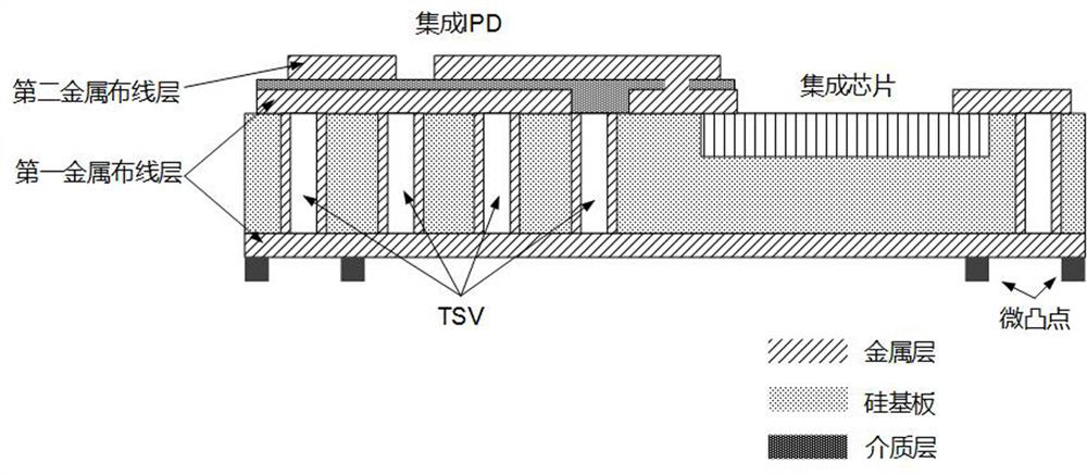
[0052] refer to figure 1 , an embodiment of the present invention provides an on-chip integrated IPD packaging structure, including:

[0053] Silicon substrate layer;

[0054] The first metal wiring layer is arranged on the upper and lower surfaces of the silicon substrate layer and communicated with through silicon vias penetrating the silicon substrate layer;

[0055] a dielectric layer disposed on the surface of the first metal wiring layer located on the upper surface of the silicon substrate layer;

[0056] The second metal wiring layer is arranged on the surface of the dielectric layer, and is sequentially stacked with the dielectric layer and the first metal wiring layer to form an on-chip integrated IPD; and

[0057] chip, integrated on the silicon substrate layer.

[0058] In this embodiment, the silicon substrate layer of the present invention adopts a commonly used silicon substrate, and for a high-frequency system, a high-resistance silicon substrate is preferab...

Embodiment 2

[0069] Based on the on-chip integrated IPD packaging structure described in Embodiment 1, an embodiment of the present invention also provides a packaging method for an on-chip integrated IPD packaging structure, including the following steps:

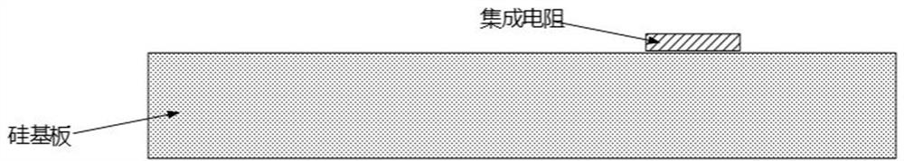
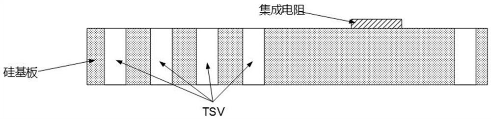
[0070] S1. Fabricate on-chip integrated resistors by sputtering on the silicon substrate layer;

[0071] S2. Fabricate through-silicon vias on the silicon substrate layer using a DRIE etching process;

[0072] S3. Sputter a seed layer on the upper and lower surfaces of the silicon substrate layer and make a photoresist mask, use a double-sided electroplating patterning process to make a continuously thickened metal layer on the upper and lower surfaces of the silicon substrate layer, and make metallized through-holes on the inner wall of the through-silicon hole. hole, remove the photoresist and seed layer to form the first metal wiring layer, including the lower electrode of the on-chip integrated inductor and on-chip integrated capac...

Embodiment 3

[0077] Based on the on-chip integrated IPD packaging structure described in Embodiment 1, the embodiment of the present invention also provides a three-dimensional packaging structure of on-chip integrated IPD, including:

[0078] Multiple single-layer on-chip integrated IPD packaging structures stacked up and down in sequence, and each on-chip integrated IPD packaging structure is interconnected through a micro-bump structure;

[0079] The on-chip integrated IPD package structure specifically includes:

[0080] Silicon substrate layer;

[0081] The first metal wiring layer is arranged on the upper and lower surfaces of the silicon substrate layer and communicated with through silicon vias penetrating the silicon substrate layer;

[0082] a dielectric layer disposed on the surface of the first metal wiring layer located on the upper surface of the silicon substrate layer;

[0083] The second metal wiring layer is arranged on the surface of the dielectric layer, and is sequen...


PUM

PropertyMeasurementUnit
thicknessaaaaaaaaaa
thicknessaaaaaaaaaa

Abstract

The invention discloses an on-chip integrated IPD packaging structure, a packaging method thereof, and a three-dimensional packaging structure. The on-chip integrated IPD packaging structure includes a silicon substrate layer, a first layer arranged on the upper and lower surfaces of the silicon substrate layer and communicated through a through-silicon hole penetrating the silicon substrate layer. A metal wiring layer, which is arranged on the dielectric layer on the surface of the first metal wiring layer on the upper surface of the silicon substrate layer, is arranged on the surface of the first dielectric layer and is sequentially stacked with the dielectric layer and the first metal wiring layer to form the first on-chip integrated IPD. Two metal wiring layers, and chips integrated on the silicon substrate layer. In the present invention, the silicon substrate is used as an integrated packaging substrate, and passive components are integrated on the substrate, and the integrated manufacturing of the packaging substrate is adopted to complete the production of components and system integration under the same process flow, without the need for separate processing and production of components. The processing integration is simple, easy to realize 3D integration, and has the advantages of high precision and good consistency, saving the circuit area and making the design more flexible.

Description

technical field [0001] The invention relates to the technical field of IPD (integrated passive device), in particular to an on-chip integrated IPD packaging structure, a packaging method thereof, and a three-dimensional packaging structure. Background technique [0002] The radio frequency system is mainly composed of amplification chips, control chips and passive components. The miniaturization and integration of passive components has attracted much attention. In the entire circuit, passive components such as inductors, capacitors, and filters account for more than 50% of the system volume, and the high-density integration and miniaturization technology of passive components has become a core issue. At present, most passive components are discrete devices, which are integrated on the pcb board by welding or bonding, requiring a large area for welding and through holes, or using LTCC substrates to integrate passive components such as inductors and capacitors, but LTCC belo...

Claims


Application Information

Patent Timeline
Patent Type & Authority Patents(China)
IPC IPC(8): H01L49/02
CPCH01L28/10H01L28/20H01L28/40
Inventor 何舒玮胡柳林陈依军卢朝保侯杰周鹏吴晓东周文瑾唐仲俊边丽菲
Owner CHENGDU GANIDE TECH
Why Eureka
Try Eureka