Photoresist collection cup structure to prevent wafer front and back side contamination

A technology of photoresist and collection cup, applied in the direction of photoplate making process coating equipment, etc., can solve the problems of polluting wafers, waste liquid polluting wafers, low yield, etc., to prevent pollution, improve yield, and simple structure Effect

Active Publication Date: 2019-07-05
SHENYANG KINGSEMI CO LTD
View PDF6 Cites 0 Cited by
  • Summary
  • Abstract
  • Description
  • Claims
  • Application Information

AI Technical Summary

Problems solved by technology

[0002] At present, in the semiconductor wafer production process, the structure of the traditional photoresist collection cup will make the waste liquid generated in the production pollute the front and back of the wafer, resulting in poor production quality and low yield. The traditional photoresist collection Cup, because the structural defect cannot solve the problem of sudden waste liquid pollution of the wafer, the quality and yield can only be guaranteed by scrapping the wafer, or reprocessing and producing the wafer after cleaning. This method is not only inefficient, but also increases the time cost and material cost of production
In order to solve the appeal problem, a new type of photoresist collection cup structure is needed to avoid the problem of waste liquid polluting the wafer during the production process

Method used


Image

  • Photoresist collection cup structure to prevent wafer front and back side contamination
  • Photoresist collection cup structure to prevent wafer front and back side contamination
  • Photoresist collection cup structure to prevent wafer front and back side contamination

Examples


Embodiment Construction

[0017] The present invention will be further described below in conjunction with the accompanying drawings.

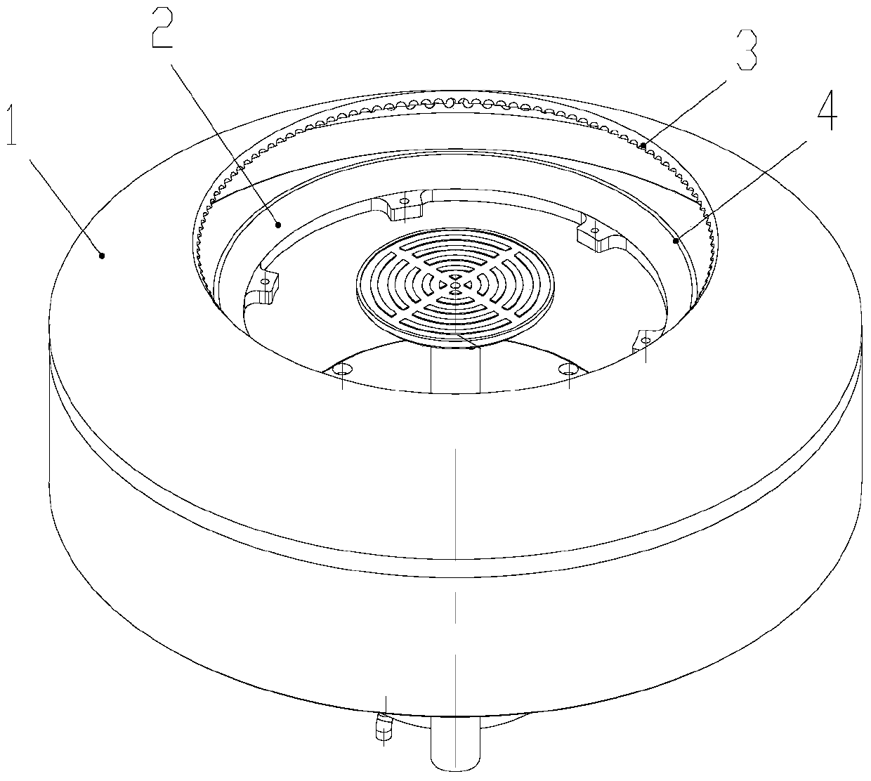
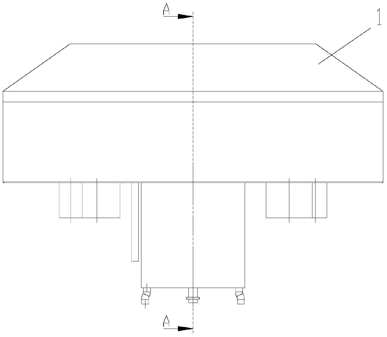
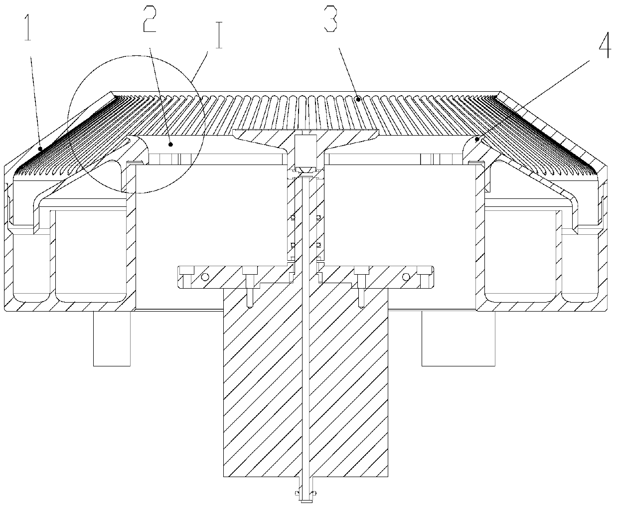
[0018] Such as Figure 1-3 As shown, the present invention includes an upper cup 1 and a lower cup 2. The inner wall of the upper cup 1 is provided with a diversion groove structure 3 for guiding the waste liquid to flow downwards, and the upper edge of the lower cup 2 is provided along the circumference to prevent waste Liquid backflow prevention structure 4.

[0019] Such as Figure 4 As shown, the diversion groove structure 3 is a plurality of side-by-side grooves that are evenly distributed on the inner wall of the upper cup 1 and arranged along the inner wall from top to bottom. The backflow preventing structure 4 is an annular retaining ring provided on the upper edge of the lower cup 2 to form a backflow preventing structure.

[0020] The working principle of the present invention is:

[0021] During the wafer production process, the excess waste liquid (pho...


PUM


Abstract

The invention relates to equipment in a semiconductor production, in particularly to a photoresist collecting cup structure for preventing the front and the back of a wafer from being polluted. The photoresist collecting cup structure comprises an upper cup and a lower cup, wherein a diversion trench structure for guiding a liquid waste to flow downwards is formed in the inner wall of the upper cup; a backflow preventing structure for preventing the liquid waste from flowing back is formed in the top edge of the lower cup along the circumferential direction; the diversion trench structure is composed of a plurality of diversion trenches which are distributed on the inner wall of the upper cup and are downward along the inner wall; and the backflow preventing structure is an annular retainer ring arranged on the top edge of the lower cup. The front and the back of the wafer are prevented from being polluted by the liquid waste generated in a gluing process when the photoresist collecting cup structure is applied to the gluing process for semiconductor production; and the yield in wafer gluing production is increased.

Description

technical field [0001] The invention relates to equipment in semiconductor production, in particular to a photoresist collection cup structure for preventing wafer front and back contamination. Background technique [0002] At present, in the semiconductor wafer production process, the structure of the traditional photoresist collection cup will cause the waste liquid generated in the production to pollute the front and back of the wafer, resulting in poor production quality and low yield. The traditional photoresist collection Cup, because the structural defect cannot solve the problem of sudden waste liquid pollution of the wafer, the quality and yield can only be guaranteed by scrapping the wafer, or reprocessing and producing the wafer after cleaning. This method is not only inefficient, but also increases the time cost and material cost of production. In order to solve the appeal problem, a new type of photoresist collection cup structure is needed to avoid the problem...

Claims


Application Information

Patent Timeline
Patent Type & Authority Patents(China)
IPC IPC(8): G03F7/16
Inventor 王阳胡延兵
Owner SHENYANG KINGSEMI CO LTD
Why Eureka
Try Eureka