
Plasma reactor and method for removing particulate contamination from plasma reaction chamber

A plasma and reaction chamber technology, used in semiconductor/solid-state device manufacturing, discharge tubes, electrical components, etc., to solve problems such as particle pollution

Active Publication Date: 2018-09-18
SEMICON MFG INT (SHANGHAI) CORP
View PDF7 Cites 0 Cited by
  • Summary
  • Abstract
  • Description
  • Claims
  • Application Information

AI Technical Summary

Problems solved by technology

[0012] The present invention aims to provide a plasma reactor and a method for removing particle pollution in the plasma reaction chamber, so as to solve the technical problem of particle pollution in the plasma reaction chamber in the prior art

Method used


Image

  • Plasma reactor and method for removing particulate contamination from plasma reaction chamber
  • Plasma reactor and method for removing particulate contamination from plasma reaction chamber

Examples


Embodiment Construction

[0031] It should be noted that, in the case of no conflict, the embodiments in the present application and the features in the embodiments can be combined with each other. The present invention will be described in detail below with reference to the accompanying drawings and examples.

[0032] A typical plasma reactor in the prior art usually includes a casing, in which there is a reaction chamber, and the top and bottom of the reaction chamber are respectively provided with an upper pole plate and a lower pole plate correspondingly. The upper pole plate and the lower pole plate are separated by an insulating part, and the top of the lower pole plate can support the workpiece to be processed. The above-mentioned processing workpieces shall include wafers and other processing workpieces with the same processing principle.

[0033] When the plasma reactor is working, a vacuum device such as a dry pump is used to create and maintain a near-vacuum state in the reaction chamber. ...


PUM


Abstract

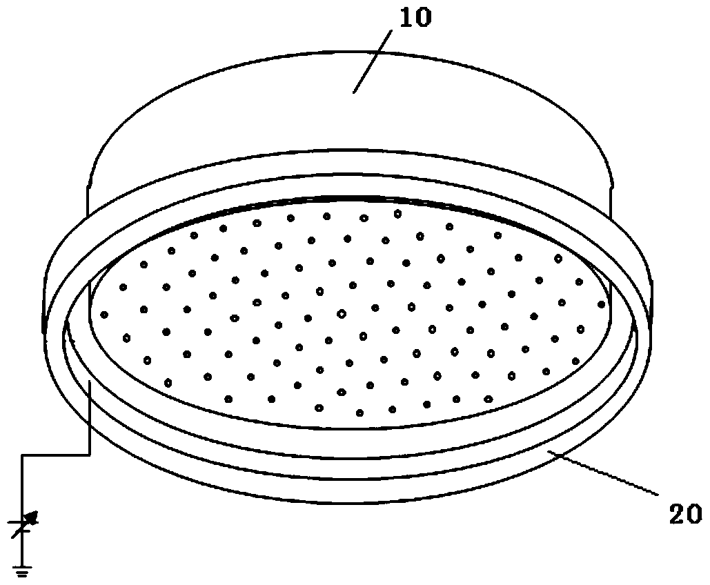
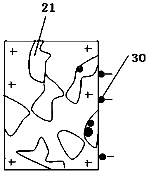
The invention discloses a plasma reactor and a method of eliminating particle pollution in a plasma reaction cavity. The plasma reactor comprises a nozzle electrode, and a device for absorbing negatively charged particles is disposed around the nozzle electrode. The method includes the step of adopting the device disposed around the nozzle electrode in a plasma reaction cavity to absorb negatively charged particles. The inventor of the invention finds that particles causing pollution in the plasma reaction cavity are mostly particles with negative electricity. Therefore, through application of the technical scheme, the device used for absorbing negatively charged particles and disposed around the nozzle electrode can effectively absorb and remove particles that cause pollution.

Description

technical field [0001] The invention relates to the technical field of semiconductor preparation, in particular to a plasma reactor and a method for removing particle pollution in a plasma reaction chamber. Background technique [0002] With the gradual increase in the integration and performance requirements of VLSI, the feature size of the device is continuously shrinking to meet the requirements of higher integration and higher performance. The existence of dust particles in the plasma reactor may cause wafer damage. Contamination, thereby seriously reducing the quality of the product obtained. In the manufacturing process of semiconductor integrated circuits, surface particle contamination is one of the important factors of yield loss, which makes it more and more critical to control surface contamination in the microelectronics manufacturing process. Among the particles that cause pollution, plasma-generated particles are the most important source of pollution. [000...

Claims


Application Information

Patent Timeline
Patent Type & Authority Patents(China)
IPC IPC(8): H01L21/00H01J37/32
Inventor 严琰童浩
Owner SEMICON MFG INT (SHANGHAI) CORP
Learn More