Method of forming contact plugs

A technology for contact plugs and contact holes, which is applied in the manufacturing of electrical components, circuits, semiconductor/solid-state devices, etc., can solve the problems of the performance of contact plugs, the difficulty of forming contact holes, and the difficulty of filling them well, so as to reduce the difficulty of forming , easy to fill, improve the quality of the effect

Active Publication Date: 2018-11-16
SEMICON MFG INT (SHANGHAI) CORP
View PDF4 Cites 0 Cited by
  • Summary
  • Abstract
  • Description
  • Claims
  • Application Information

AI Technical Summary

Problems solved by technology

However, forming a contact hole 111 with a large depth and a relatively steep inner wall is undoubtedly a major challenge in the industry. What's more, even if the contact hole 111 with a large depth and a steep inner wall is successfully formed, it is extremely difficult to fill. Some methods have been difficult to fill it well, resulting in the performance degradation of the final contact plug
[0006] For this reason, a new method of forming contact plugs is needed to solve the problem that contact holes are difficult to form in the existing methods, and even after being formed, it is still difficult to fill them well, resulting in the degradation of the performance of contact plugs.

Method used


Image

  • Method of forming contact plugs
  • Method of forming contact plugs
  • Method of forming contact plugs

Examples


Embodiment Construction

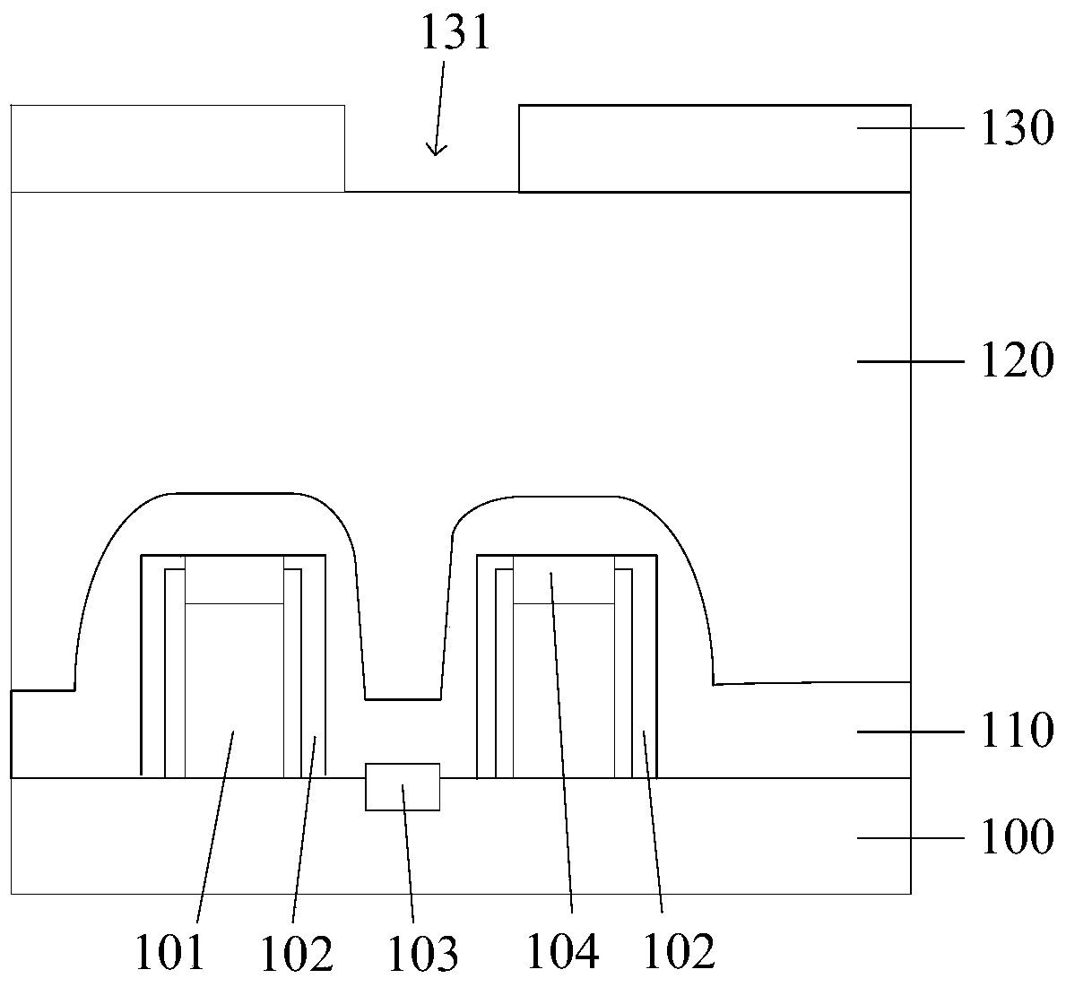
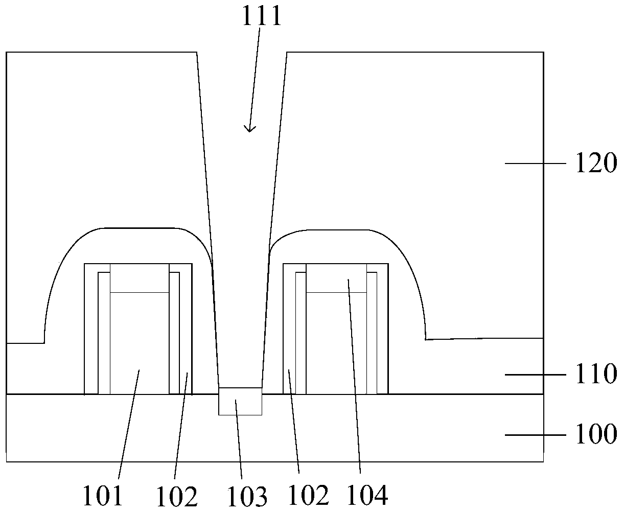
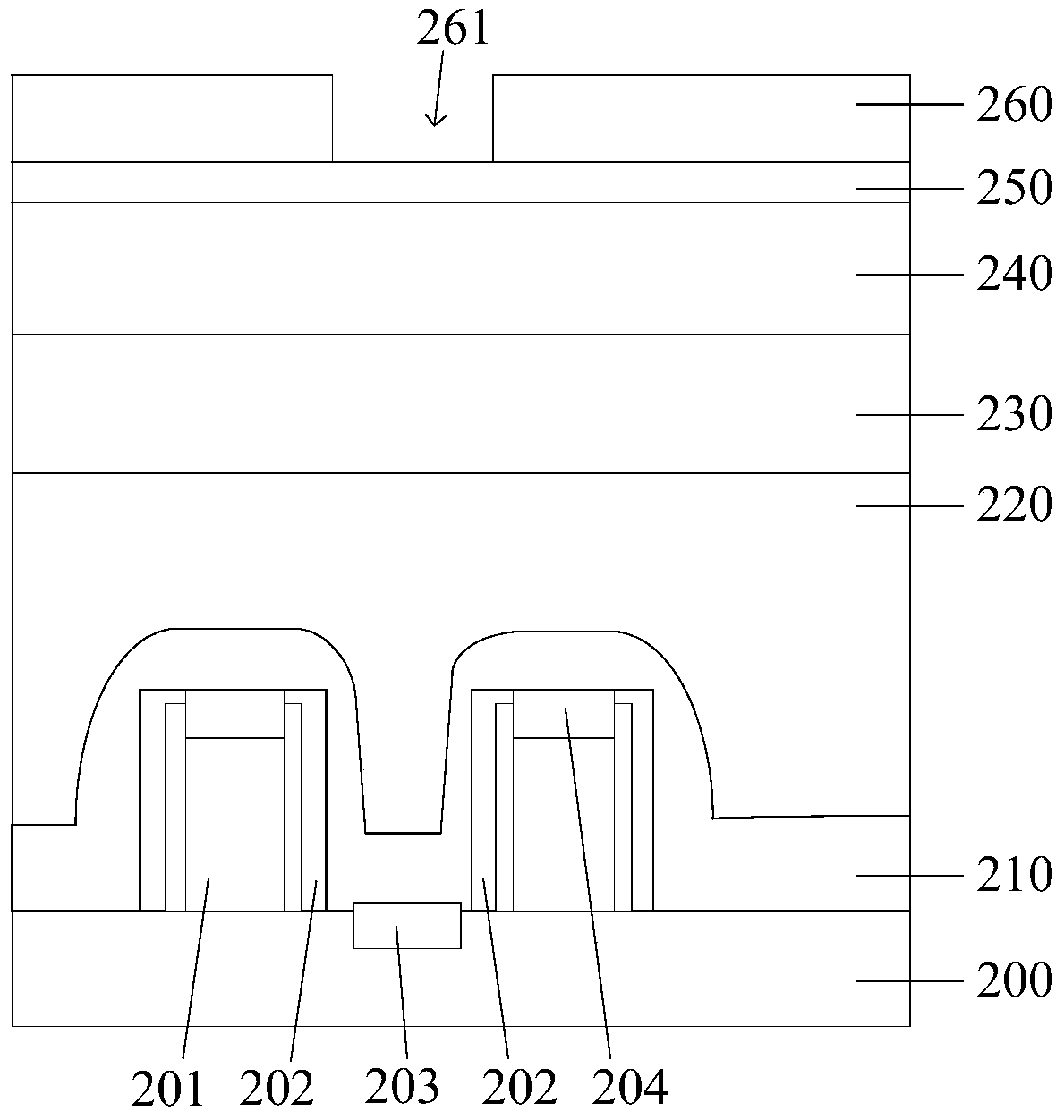
[0036] It is generally believed in the industry that in order to avoid the potential bright voltage contrast problem and also to avoid the distance between the gate structure and the formed conductive plug being too small, it is necessary to make a contact hole with a large depth and a relatively steep inner wall. However, forming a contact hole with a large depth and a relatively steep inner wall is undoubtedly a major challenge in the industry, and the contact hole with a large depth and a relatively steep inner wall also brings great difficulties to the subsequent filling process.

[0037] After analysis, it is found that it is only necessary to ensure that the steep part of the inner wall of the contact hole is higher than the gate structure by a certain height, and the entire inner wall of the contact hole does not need to have a steep structure.

[0038]To this end, the present invention provides a new method for forming a contact plug, which adds a high-K dielectric laye...


PUM


Abstract

A formation method of a contact plug comprises the steps of providing a substrate; forming an interlayer dielectric layer on the substrate; forming a high K dielectric layer on the interlayer dielectric layer; etching the high K dielectric layer and the interlayer dielectric layer orderly until the substrate is exposed to form a contact hole; continuously etching the high K dielectric layer along the contact hole until the diameter of the contact hole located at the high K dielectric layer is increased; adopting a conductive material to fill the contact hole. The formation method of the contact plug enables the formation difficulty of the contact plug to be reduced and also the quality of the formed contact plug to be improved.

Description

technical field [0001] The invention relates to the field of semiconductor manufacturing, in particular to a method for forming a contact plug. Background technique [0002] In the integrated circuit manufacturing process, in order to connect semiconductor devices such as CMOS on the semiconductor substrate with the upper metal interconnection layer, a metal pre-dielectric layer between the first metal interconnection layer and the semiconductor device layer ( Inter-metal Dielectric, IMD) etch to form a contact hole, and then fill the contact hole with (metal) conductive material such as tungsten, aluminum or copper to form a contact plug (contact). [0003] Please refer to figure 1 , the conventional method for forming a contact plug generally includes: providing a substrate 100 with a MOS transistor on the substrate 100, the MOS transistor includes a gate structure 101, sidewalls 102 positioned on the sides of the gate structure, and a metal layer in the substrate below t...

Claims


Application Information

Patent Timeline
Patent Type & Authority Patents(China)
IPC IPC(8): H01L21/768
Inventor 张海洋黄敬勇何其暘
Owner SEMICON MFG INT (SHANGHAI) CORP
Why Eureka
Try Eureka