

Semiconductor structure forming method
A semiconductor and gas technology, applied in semiconductor/solid-state device manufacturing, electrical components, circuits, etc., can solve the problems of semiconductor structure yield to be improved, semiconductor structure performance, etc., to avoid undercutting, optimize performance, and avoid undercutting problem-solving effect
- Summary
- Abstract
- Description
- Claims
- Application Information
AI Technical Summary
Problems solved by technology
Method used
Image

Examples
Embodiment Construction
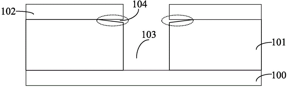
[0033] It can be seen from the background art that the performance of the semiconductor structure formed in the prior art needs to be improved, and the yield rate of the semiconductor structure is poor.
[0034] Please refer to figure 1 The step of forming the semiconductor structure includes: providing a substrate 100; forming a dielectric layer 101 on the surface of the substrate 100; forming a patterned hard mask layer 102 on the surface of the dielectric layer 101; The film layer 102 is used as a mask to etch the dielectric layer 101 to form an opening 103 in the dielectric layer 101 ; the subsequent steps include filling the opening 103 with a metal material.
[0035] In order to reduce the RC delay of the semiconductor structure, a low-k dielectric material or an ultra-low-k dielectric material is usually used as the material of the dielectric 101, and the low-k dielectric material or the ultra-low-k dielectric material usually contains a methyl group (-CH 3 ), that is,...
PUM
| Property | Measurement | Unit |
|---|---|---|
| thickness | aaaaa | aaaaa |
| thickness | aaaaa | aaaaa |
| thickness | aaaaa | aaaaa |
Abstract
Description
Claims
Application Information