Salient point structure for preventing salient point lateral etching and forming method

A technology of lateral etching and forming methods, which is applied in the direction of electrical components, electrical solid devices, circuits, etc., can solve the problems of control limitations of the etching process, and achieve the effect of avoiding lateral undercutting

Active Publication Date: 2014-06-25
NAT CENT FOR ADVANCED PACKAGING
View PDF5 Cites 8 Cited by
  • Summary
  • Abstract
  • Description
  • Claims
  • Application Information

AI Technical Summary

Problems solved by technology

Due to the problem of undercutting, the selection of etching solution and the control of etching process will be limited when etching the seed layer

Method used


Image

  • Salient point structure for preventing salient point lateral etching and forming method
  • Salient point structure for preventing salient point lateral etching and forming method
  • Salient point structure for preventing salient point lateral etching and forming method

Examples


Embodiment Construction

[0036] The present invention will be further described below in conjunction with specific drawings and embodiments.

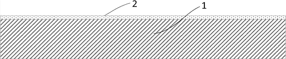
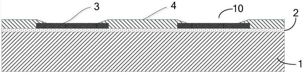
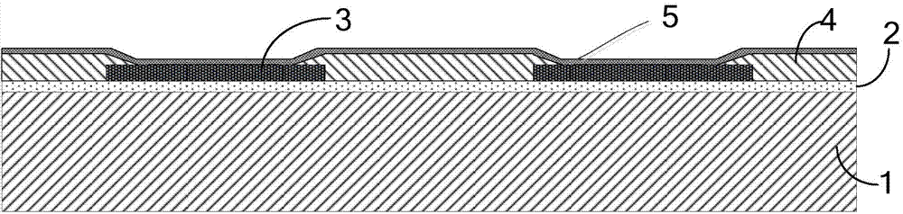
[0037] Such as Figure 10 Shown: In order to avoid the phenomenon of undercutting and improve the reliability and yield rate of micro-bump manufacturing, the present invention includes a substrate 1 and an insulating layer 2 located on the substrate 1; on the insulating layer 2 A metal pad 3 is provided, and the outer ring of the metal pad 3 is provided with a dielectric layer 4, and the dielectric layer 4 covers the insulating layer 2 and covers the edge of the outer ring of the metal pad 3; the metal pad 3 A copper post 8 is provided directly above the copper post 8, and the bottom end of the copper post 8 contacts and is electrically connected to the metal pad 3 through the seed layer 6 and the adhesive layer 5 in turn, and the bottom end of the copper post 8 passes through the seed layer 6 and the adhesive layer 5. The attachment layer 5 is supported on th...


PUM


Abstract

The invention relates to a semiconductor structure and manufacturing method thereof, in particular to a salient point structure for preventing salient point lateral etching and a forming method and belongs to the technical field of semiconductor manufacturing. In the technical scheme, the salient point structure for preventing the salient point lateral etching comprises a substrate and an insulating layer located on the substrate. A metal bonding pad is arranged on the insulating layer, an outer ring of the metal bonding pad is provided with a dielectric layer, the dielectric layer covers the insulating layer and the edge of the outer ring of the metal bonding pad. A copper column is arranged right above the metal bonding pad, the bottom end of the copper column sequentially passes through a seed layer and an adhesion layer to be in contact with and electrically connected with the metal bonding pad and is supported on the dielectric layer through the seed layer and the adhesion layer, and welding flux salient points are arranged at the top end of the copper column. The salient point structure for preventing the salient point lateral etching adopts a method for firstly imaging the adhesion layer, the problem that the lateral etching is easily caused during adhesion layer removal after electroplating is solved, and the reliability and yield of machined and manufactured salient points are improved.

Description

technical field [0001] The invention relates to a semiconductor structure and a preparation method thereof, in particular to a bump structure and a molding method for preventing lateral etching of bumps, and belongs to the technical field of semiconductor manufacturing. Background technique [0002] Traditionally, the electrical connection between the IC chip and the outside is achieved by bonding the I / O on the chip to the package carrier through metal wires through the package pins. With the reduction of IC chip feature size and the expansion of integration scale, the pitch of I / O is decreasing and the number is increasing. When the I / O pitch is reduced below 70 μm, the wire bonding technology is no longer applicable, and new technical approaches must be sought. [0003] Wafer-level packaging technology uses thin film redistribution technology, so that I / O can be distributed on the entire surface of the IC, rather than limited to the peripheral area of ​​​​the narrow IC c...

Claims


Application Information

Patent Timeline
Patent Type & Authority Applications(China)
IPC IPC(8): H01L23/498H01L21/48
CPCH01L24/11H01L2224/11H01L2224/11462H01L2224/1147H01L2224/11849H01L2224/13H01L2224/13082H01L2224/131H01L2224/13147H01L2924/014H01L2924/00014H01L2924/00012
Inventor 李昭强戴风伟于大全
Owner NAT CENT FOR ADVANCED PACKAGING
Why Eureka
Try Eureka