Fabrication method of low-temperature polycrystalline silicon thin-film transistor (TFT) substrate structure and low-temperature polycrystalline silicon TFT substrate structure

一种低温多晶硅、制作方法的技术,应用在半导体/固态器件制造、半导体器件、电气元件等方向,能够解决晶粒一致性和晶粒的大小不能做到有效控制、驱动TFT电性一致性和电性稳定性差、多晶硅晶粒一致性差等问题,达到避免画质不良、电性稳定性好、晶粒一致性好的效果

Active Publication Date: 2015-11-25
TCL CHINA STAR OPTOELECTRONICS TECH CO LTD
View PDF12 Cites 9 Cited by
  • Summary
  • Abstract
  • Description
  • Claims
  • Application Information

AI Technical Summary

Problems solved by technology

[0005] However, the current ELA crystallization technology cannot effectively control the consistency and size of the crystal grains, so the crystallization status is very unevenly distributed on the entire substrate, resulting in poor consistency of the polysilicon crystal grains in the driving TFT area, and The crystal grains are relatively small, which makes the electrical consistency and electrical stability of the driving TFT poor, which easily leads to poor image quality and other phenomena.

Method used


Image

  • Fabrication method of low-temperature polycrystalline silicon thin-film transistor (TFT) substrate structure and low-temperature polycrystalline silicon TFT substrate structure
  • Fabrication method of low-temperature polycrystalline silicon thin-film transistor (TFT) substrate structure and low-temperature polycrystalline silicon TFT substrate structure
  • Fabrication method of low-temperature polycrystalline silicon thin-film transistor (TFT) substrate structure and low-temperature polycrystalline silicon TFT substrate structure

Examples


Embodiment Construction

[0037] In order to further illustrate the technical means adopted by the present invention and its effects, the following describes in detail in conjunction with preferred embodiments of the present invention and accompanying drawings.

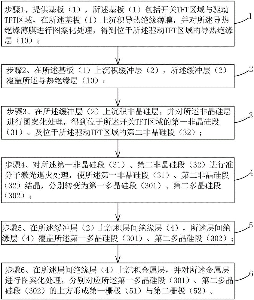
[0038] see figure 1 , the present invention at first provides a kind of fabrication method of low-temperature polysilicon TFT substrate structure, comprises the following steps:

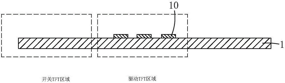
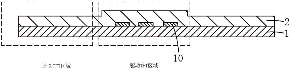
[0039] Step 1, such as figure 2 As shown, a substrate 1 is provided. The substrate 1 includes a switching TFT area and a driving TFT area. A thermally conductive insulating film is deposited on the substrate 1, and the thermally conductive insulating film is patterned to obtain a TFT located in the driving TFT area. The thermally conductive insulating layer 10.

[0040] Specifically, the substrate 1 may be a glass substrate or a silicon substrate.

[0041] Specifically, the material of the thermally conductive insulating layer 10 is magnesium oxide or aluminum ox...


PUM


Abstract

The invention provides a fabrication method of a low-temperature polycrystalline silicon thin-film transistor (TFT) substrate structure and the low-temperature polycrystalline silicon TFT substrate structure. According to the fabrication method of the low-temperature polycrystalline silicon TFT substrate structure provided by the invention, patterns, which are consistent in law and size, of heat-conducting insulating layers are arranged below a buffer layer of a drive TFT region; the heat-conducting insulating layers absorb heat in the subsequent excimer laser annealing treatment process, so that the cooling speed of amorphous silicon is quickened to form crystal nucleus; the crystal nucleus gradually grows in the annealing process; the heat-conducting insulating layers have the patterns which are consistent in law and size, so that polycrystalline silicon grains formed by the drive TFT region have relatively good consistency; the grains are relatively large; and the electrical consistency of a drive TFT is ensured. According to the low-temperature polycrystalline silicon TFT substrate structure provided by the invention, the patterns, which are consistent in law and size, of the heat-conducting insulating layers are arranged below the buffer layer of the drive TFT region; the polycrystalline silicon grains of the drive TFT region are relatively good in consistency and relatively large; and the electrical consistency of the drive TFT is relatively good.

Description

technical field [0001] The invention relates to the field of display technology, in particular to a method for manufacturing a low-temperature polysilicon TFT substrate structure and a low-temperature polysilicon TFT substrate structure. Background technique [0002] Low-temperature polysilicon (LowTemperaturePoly-silicon, LTPS) thin film transistor (ThinFilmTransistor, TFT) has great application value and potential in the field of high-resolution active liquid crystal display (ActiveMatrixLiquidCrystalDisplay, AMLCD) and organic light-emitting diode (Active-MatrixOrganicLightEmittingDiode, AMOLED) display . [0003] Compared with amorphous silicon (a-Si) technology, LTPSTFT has high mobility and good device stability. The mobility of LTPSTFT can reach tens to hundreds of cm 2 / Vs, which can meet the requirements of high-resolution AMLCD and AMOLED displays. Therefore, the low-temperature polysilicon display has a faster response speed, and has the advantages of high brig...

Claims


Application Information

Patent Timeline
Patent Type & Authority Applications(China)
IPC IPC(8): H01L21/77H01L27/12
CPCH01L27/1218H01L27/1262H01L27/1296H01L27/1229H01L27/1274H01L27/1281H01L27/1285H01L21/02532H01L21/02592H01L21/0262H01L21/02667H01L21/02672H01L21/02675
Inventor 张良芬
Owner TCL CHINA STAR OPTOELECTRONICS TECH CO LTD
Why Eureka
Try Eureka