Formation method of package structure

A technology of packaging structure and plastic sealing layer, which is applied in the direction of electrical components, electric solid devices, circuits, etc., can solve the problem of reducing the thickness and size of the packaging structure, and achieve the effect of accurate relative position, fixed and stable

Active Publication Date: 2017-12-08
NANTONG FUJITSU MICROELECTRONICS
View PDF4 Cites 0 Cited by
  • Summary
  • Abstract
  • Description
  • Claims
  • Application Information

AI Technical Summary

Problems solved by technology

[0006] However, the above-mentioned technical means still face various process constraints and cost constraints, and face the problem of further reducing the thickness of the packaging structure

Method used


Image

  • Formation method of package structure
  • Formation method of package structure
  • Formation method of package structure

Examples


Embodiment Construction

[0042] As mentioned in the background technology, the existing stacked chip packaging technology faces process limitations and cost constraints, which limits the popularization and application of the technology. Moreover, the stacked chip packaging technology is also facing the problem of further reducing the thickness of the packaging structure, in order to further Improve chip integration and reduce size.

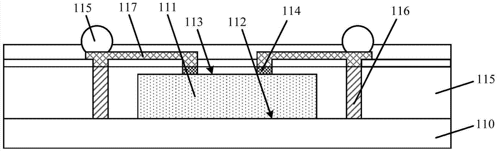
[0043] The stacked chip packaging technology can be realized through a through silicon via (TSV for short) technology or a through molding via (TMV for short) technology. However, both the TSV technology and the TSV technology have certain defects.

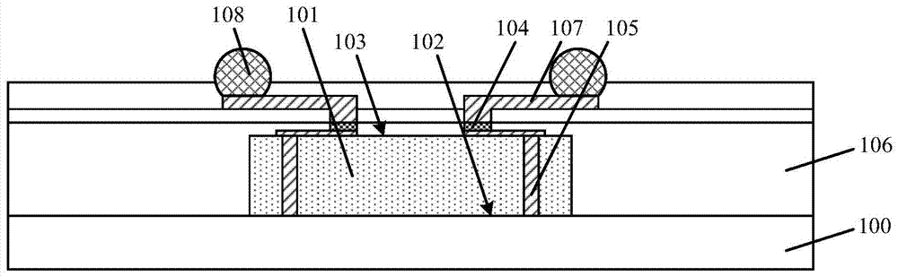
[0044] Please refer to figure 1 , figure 1It is a schematic cross-sectional structure diagram of introducing a through-silicon via structure in the packaging structure to realize the conduction between chips, including: a carrier 100; a chip 101 fixed on the surface of the carrier 100, and the chip 101 includes an opposite ...


PUM


Abstract

A method for forming a packaging structure, comprising: providing a carrier having a chip area, an opposite third surface, and a fourth surface; forming a slot around the chip area in the carrier; fixing a chip on the third surface of the carrier chip area, The chip has an opposite first surface and a second surface, the second surface of the chip includes a functional area, the first surface of the chip and the third surface of the carrier are fixed to each other; the connecting key including the first end and the second end is fixed in the slot , the first end and the second end of the connection key expose conductive wires, the first end of the connection key is located in the slot, and the second end of the connection key is flush with the surface of the functional area of ​​the chip; a surrounding area is formed on the third surface of the carrier The plastic encapsulation layer of the chip and the connection key; thinning the fourth surface of the carrier until the second end of the connection key is exposed; forming a rewiring layer and the first solder ball on the surface of the plastic encapsulation layer. The forming method of the packaging structure is simple, the process cost is reduced, and the size of the formed packaging structure is accurate and reduced.

Description

technical field [0001] The invention relates to the technical field of semiconductor manufacturing, in particular to a method for forming a packaging structure. Background technique [0002] In the prior art, the connection between the chip and the external circuit is realized by metal wire bonding (Wire Bonding), that is, wire bonding technology. With the reduction of chip feature size and the improvement of integrated circuit integration, wire bonding technology is no longer applicable to the development needs of technology. [0003] In order to improve the integration level of chip packaging, stacked die package (stacked die package) technology has gradually become the mainstream of technology development. Stacked chip packaging technology, also known as three-dimensional packaging technology, is specifically a packaging technology that stacks at least two chips in the same package. Stacked chip packaging technology can meet the technical requirements of semiconductor d...

Claims


Application Information

Patent Timeline
Patent Type & Authority Patents(China)
IPC IPC(8): H01L23/13H01L23/498H01L23/49H01L21/56H01L21/60
CPCH01L24/19H01L2224/04105H01L2224/12105H01L2224/19H01L2224/20H01L2224/32225H01L2224/48091H01L2224/48227H01L2224/73265H01L2224/73267H01L2224/92244H01L2225/1035H01L2225/1041H01L2225/1058H01L2924/15311H01L2924/181H01L2924/00012H01L2924/00014H01L2924/00
Inventor 石磊
Owner NANTONG FUJITSU MICROELECTRONICS
Why Eureka
Try Eureka