Unlock instant, AI-driven research and patent intelligence for your innovation.
Photoresist, quantum dot layer patterning method, quantum light-emitting diode (QLED), quantum dot color film and display device
What is Al technical title?
Al technical title is built by PatSnap Al team. It summarizes the technical point description of the patent document.
A technology of quantum dot layer and photoresist, which is applied in the direction of electrical components, circuits, semiconductor devices, etc., and can solve the problem of destroying quantum dots
Active Publication Date: 2015-11-25
BOE TECH GRP CO LTD
View PDF5 Cites 11 Cited by
Summary
Abstract
Description
Claims
Application Information
AI Technical Summary
This helps you quickly interpret patents by identifying the three key elements:
Problems solved by technology
Method used
Benefits of technology
Problems solved by technology
[0006] The present invention aims at the problem that the existing patterning method destroys the quantum dot, and provides a method for patterning the quantum dot layer
Method used
Image
Click on the blue label to locate the original text in one second.
Reading with bidirectional positioning of images and text.
Examples
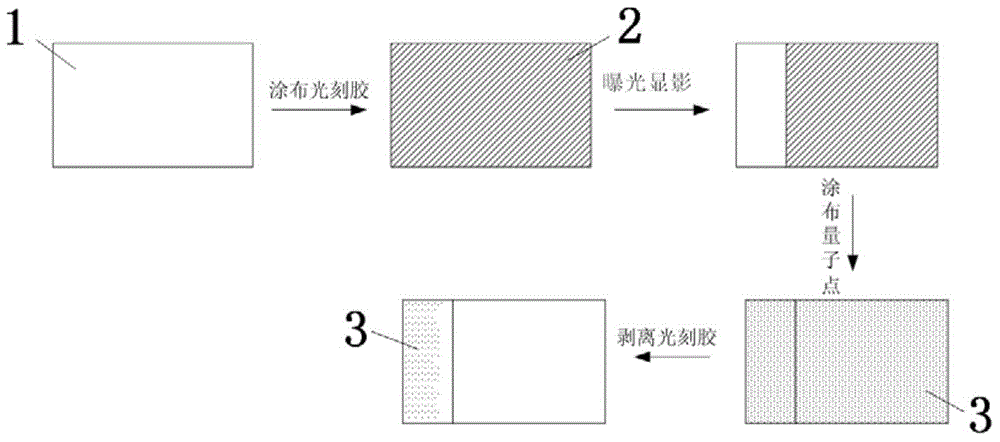
Embodiment 1
[0048] This embodiment provides a method for patterning a quantum dot layer, comprising the following steps:
[0049] The step of forming a photoresist material layer on the substrate, the step of patterning the photoresist, and the step of hydrophilically treating the photoresist;
[0051] a step of removing the quantum dots on the remaining photoresist;
[0052] The step of stripping the photoresist.
[0053] Wherein, the step of forming a photoresist material layer on the substrate, the step of patterning the photoresist, and the step of hydrophilically treating the photoresist, the steps are not limited in sequence;
[0054] The step of hydrophilically treating the photoresist may be performed after forming the photoresist material layer and before patterning, or after forming the photoresist material layer and patterning.
[0055] In the quantum dot layer patterning method of the present embodiment, comprise the step of carryi...
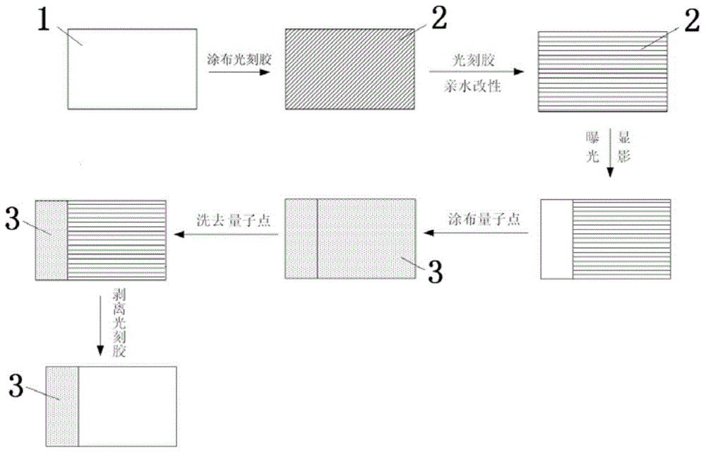
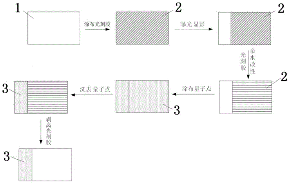
Embodiment 2
[0057] This embodiment provides a method for patterning a quantum dot layer, such as Figure 2-4 shown, including the following steps:
[0058] A step of forming a photoresist 2 material layer on the substrate 1, a step of patterning the photoresist 2, and a step of hydrophilically treating the photoresist 2;
[0060] a step of removing the quantum dots on the remaining photoresist;
[0061] Step of stripping photoresist 2.
[0062] That is to say, in this embodiment, the photoresist 2 is subjected to hydrophilic treatment to improve the hydrophilic property of the photoresist 2 .
[0063]The schematic diagram of the structure of quantum dot 3 is shown in Figure 4 As shown, the quantum dot 3 is composed of three parts, namely a luminescent core 31, a semiconductor shell 32, and an organic ligand 33; the organic ligand 33 includes a lipophilic group, such as oleylamine CH 3 (CH 2 ) 7 CH=CH(CH 2 ) 7 CH 2 NH 2 , or oleic CH ...
Embodiment 3
[0097] This embodiment provides a photoresist for patterning a quantum dot layer, and the photoresist contains a hydrophilic group.
PUM
Abstract
The invention provides a photoresist, a quantum dot layer patterning method, a quantum light-emitting diode (QLED), a quantum dot color film and a display device, which belongs to the technical field of display and can be used for solving the problem of quantum dot damage by the traditional patterning method. The quantum dot layer patterning method comprises the following steps of: forming a photoresist material layer on a substrate; carrying out pattern composition on the photoresist; carrying out hydrophilic treatment on the photoresist; coating quantum dots; removing the quantum dots on the residual photoresist; and stripping the photoresist. By the quantum dot layer patterning method, the hydrophilic performance of the photoresist can be improved, and the adhesive force of the quantum dots with lipophilicity onto the photoresist is reduced. During stripping the photoresist, the quantum dots at the target position of the substrate cannot fall off. The quantum dot layer patterning method is suitable for a light-emitting diode displayer containing the quantum dot layer, the quantum dot color film and the display device applying the quantum dot color film.
Description
technical field [0001] The invention belongs to the field of display technology, and in particular relates to a photoresist, a method for patterning a quantum dot layer, a QLED, a quantum dot color film and a display device. Background technique [0002] Quantum Dot (QD), also known as nanocrystal, is a nanoparticle composed of II-VI or III-V elements. Since electrons and holes are quantum-confined, the continuous energy band structure becomes The discrete energy level structure with molecular characteristics can emit fluorescence after being excited, and its luminescence spectrum can be controlled by changing the size of quantum dots. The fluorescence intensity and stability are very good, and it is a good electroluminescent material. [0003] At present, quantum dots have been widely used in the display field as a display material, for example, quantum dot light-emitting diodes (QLEDs) manufactured by using quantum dots as light-emitting materials for the light-emitting la...
Claims
Application Information
Patent Timeline
Application Date:The date an application was filed.
Publication Date:The date a patent or application was officially published.
First Publication Date:The earliest publication date of a patent with the same application number.
Issue Date:Publication date of the patent grant document.
PCT Entry Date:The Entry date of PCT National Phase.
Estimated Expiry Date:The statutory expiry date of a patent right according to the Patent Law, and it is the longest term of protection that the patent right can achieve without the termination of the patent right due to other reasons(Term extension factor has been taken into account ).
Invalid Date:Actual expiry date is based on effective date or publication date of legal transaction data of invalid patent.

