Method for manufacturing electroplating seed layer

A manufacturing method and seed layer technology, applied in coatings, circuits, sputter plating, etc., can solve the problems of disconnection of the electroplating seed layer, poor deposition of the bottom of the contact hole, poor continuity of the electroplating seed layer, etc., to ensure electrical conductivity efficiency, improve performance, and ensure continuity and uniformity

Inactive Publication Date: 2015-12-02
CHENGDU HIWAFER SEMICON CO LTD
View PDF5 Cites 0 Cited by
  • Summary
  • Abstract
  • Description
  • Claims
  • Application Information

AI Technical Summary

Problems solved by technology

However, when the existing electroless metal plating technology deposits an electroplating seed layer on a semiconductor device with a contact hole on the back, the electroplating seed layer is well deposited on the surface of the semiconductor device and the hole wall of the contact hole, and the coverage is uniform, but at the bottom of the contact hole

Method used


Image

  • Method for manufacturing electroplating seed layer
  • Method for manufacturing electroplating seed layer

Examples


Embodiment Construction

[0014] The following will clearly and completely describe the technical solutions in the embodiments of the present invention with reference to the accompanying drawings in the embodiments of the present invention. Obviously, the described embodiments are only some, not all, embodiments of the present invention. Based on the embodiments of the present invention, all other embodiments obtained by persons of ordinary skill in the art without making creative efforts belong to the protection scope of the present invention.

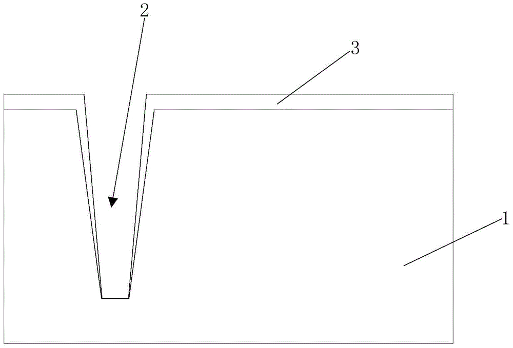
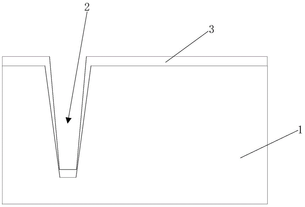
[0015] Please refer to figure 1 and figure 2 , the embodiment of the present invention provides a method for manufacturing an electroplating seed layer. In this embodiment, the manufacturing method is used for a semiconductor device 1. The surface of the semiconductor device 1 has at least one contact hole 2, and the bottom of the contact hole 2 is metal. The production method includes:

[0016] S1: An electroplating seed layer 3 is deposited on the surface...


PUM


Abstract

The invention provides a method for manufacturing an electroplating seed layer. The function of the electroplating seed layer lies in that a good conducting layer is provided for the subsequent metal electroplating technology. The manufacturing method is used for a semiconductor device. At least one contact hole is formed in the surface of the semiconductor device, and the hole bottoms of the contact holes are made of metal. The manufacturing method includes the steps that the electroplating seed layer is deposited on the surface of the semiconductor device through the chemical metal coating technology, and covers the surface of the semiconductor device and the hole walls and the hole bottoms of the contact holes; the deposition thickness of the positions, located on the hole bottoms of the contact holes, of the electroplating seed layer is increased through the metal vacuum evaporation process, so that the electroplating seed layer completely covers the hole bottoms of the contact holes. In this way, the phenomenon that the hole bottoms of the contact holes of the electroplating seed layer are disconnected can be prevented.

Description

technical field [0001] The invention relates to the field of semiconductor surface electroplating, in particular to a method for preparing an electroplating seed layer. Background technique [0002] In the semiconductor manufacturing process, the metal plating process has excellent characteristics such as simple process, low cost, fast deposition speed, and good uniformity. However, when the existing electroless metal plating technology deposits an electroplating seed layer on a semiconductor device with a contact hole on the back, the electroplating seed layer is well deposited on the surface of the semiconductor device and the hole wall of the contact hole, and the coverage is uniform, but at the bottom of the contact hole Poor deposition results in poor continuity of the electroplating seed layer, and the electroplating seed layer is prone to disconnection, which will directly affect the subsequent metal electroplating process, resulting in poor conductivity of the contac...

Claims


Application Information

Patent Timeline
IPC IPC(8): C25D7/12C23C18/31C23C14/24C23C14/16C23F17/00
Inventor 韩志龙陈汝钦
Owner CHENGDU HIWAFER SEMICON CO LTD
Why Eureka
Try Eureka