Method for modifying hole wall of zero-mode waveguide hole and structure of zero-mode waveguide hole

A zero-mode waveguide and modification method technology is applied in the field of zero-mode waveguide hole structure and zero-mode waveguide hole wall modification, which can solve the problems of fluorescence signal detection interference, nucleotides, fluorescence quenching, etc. Free nucleotides, sensitive detection, enhanced fluorescence effect

Active Publication Date: 2022-03-08
SUZHOU INST OF BIOMEDICAL ENG & TECH CHINESE ACADEMY OF SCI
View PDF6 Cites 0 Cited by
  • Summary
  • Abstract
  • Description
  • Claims
  • Application Information

AI Technical Summary

Problems solved by technology

[0004] However, during the sequencing process, there are many free nucleotides in the pores, which interfere with the detection of fluorescent signals and cause low signal-to-noise ratios; the closer the fluorescence is excited to the metal pore wall, the weaker the effect will be, and it will occur when it is completely close fluorescence quenching

Method used


Image

  • Method for modifying hole wall of zero-mode waveguide hole and structure of zero-mode waveguide hole
  • Method for modifying hole wall of zero-mode waveguide hole and structure of zero-mode waveguide hole
  • Method for modifying hole wall of zero-mode waveguide hole and structure of zero-mode waveguide hole

Examples


Embodiment Construction

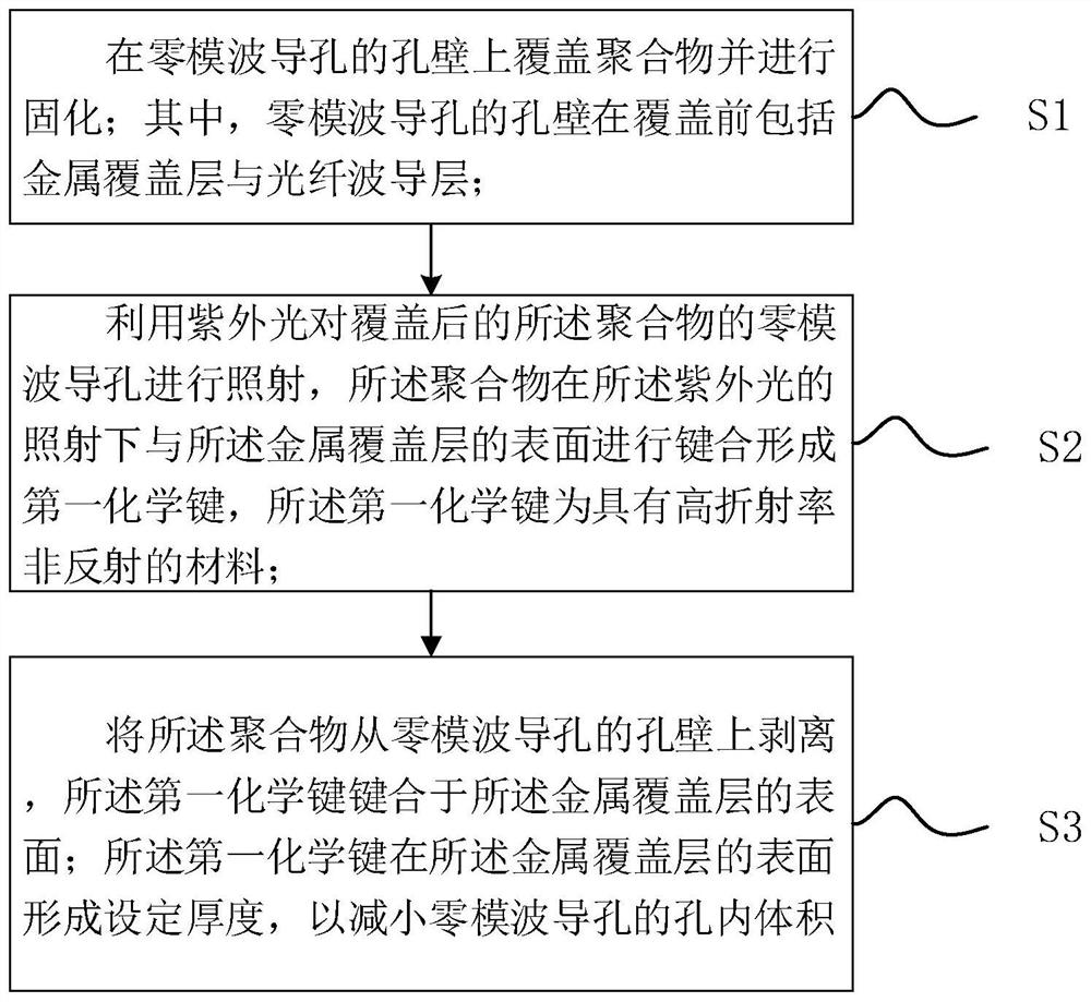
[0036] Below, the present invention will be further described in conjunction with the accompanying drawings and specific implementation methods. It should be noted that, under the premise of not conflicting, the various embodiments described below or the technical features can be combined arbitrarily to form new embodiments. .

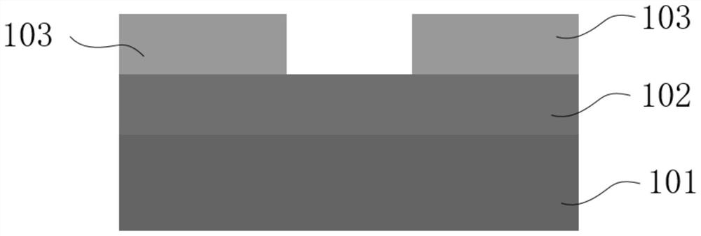
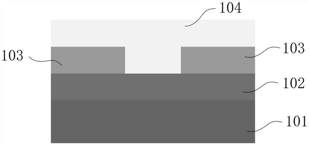
[0037] The invention provides a method for modifying the wall of a zero-mode waveguide hole, such as Figure 1-6 shown, including the following steps:

[0038] S1. Cover the hole wall of the zero-mode waveguide hole with a polymer 104 and cure it; wherein, the hole wall of the zero-mode waveguide hole includes a metal cladding layer 103 and an optical fiber waveguide layer 102 before covering. In one embodiment, such as figure 2 , 3 As shown, the metal cladding layer 103 and the optical fiber waveguide layer 102 form a hole whose wall is the hole of the metal cladding layer 103 and whose bottom end is the hole of the optical fiber waveguide layer 1...


PUM

PropertyMeasurementUnit
wavelengthaaaaaaaaaa
diameteraaaaaaaaaa

Abstract

The invention provides a method for modifying the wall of a zero-mode waveguide hole, which includes covering polymer, irradiating ultraviolet light to form a first chemical bond on the surface of the metal covering layer, and peeling off the polymer. The invention also relates to a zero-mode waveguide hole structure. In the present invention, the polymer is covered on the hole wall of the zero-mode waveguide hole, and the surface of the metal coating layer is irradiated by ultraviolet light to bond to form a first chemical bond with a high refractive index non-reflection; increase the high refractive index non-reflective material The deposition thickness of the first chemical bond can reduce the volume in the hole of the zero-mode waveguide hole, significantly reduce the free nucleotides in the hole, and improve the signal-to-noise ratio. In addition, by depositing the first chemical bond of a high-refractive index non-reflective material inside the hole, the position of the excited fluorescence can be kept away from the metal wall of the zero-mode waveguide hole, so that the fluorescence will not be weakened or even quenched. more sensitive.

Description

technical field [0001] The invention relates to the field of micro-nano processing technology, in particular to a method for modifying the hole wall of a zero-mode waveguide hole and a zero-mode waveguide hole structure. Background technique [0002] Currently, real-time single-molecule sequencing is achieved using zero-mode waveguide pores (ZMW). are fluorescently labeled phosphate-linked nucleotides that allow visualization of uninterrupted DNA polymerization. [0003] ZMWs nanostructures consist of dense arrays of holes deposited on transparent substrates such as silicon dioxide. Each ZMW becomes a nanophotonic visualization chamber for recording a single polymerization reaction, offering a detection volume of only 10 -21 Lift. This volume is a 1000-fold improvement over diffraction-limited confocal microscopy, enabling the visualization of single nucleotide incorporation events in the context of diffusion of fluorescently labeled nucleotides. In addition to reducing ...

Claims


Application Information

Patent Timeline
Patent Type & Authority Patents(China)
IPC IPC(8): G02B6/10G02B6/13C12M1/00C12Q1/6869
CPCG02B6/107G02B6/13C12Q1/6869C12Q2565/631
Inventor 周连群付博文郭振李传宇李金泽张威李超姚佳张芷齐
Owner SUZHOU INST OF BIOMEDICAL ENG & TECH CHINESE ACADEMY OF SCI
Why Eureka
Try Eureka