

Preparation method of TEM (Transmission Electron Microscope) sample
A sample and chip technology, applied in the field of shallow trench isolation structure manufacturing, can solve the problems of high difficulty, low productivity, high cost, etc., and achieve simple, cost-effective, high-efficiency, and low-cost effects
- Summary
- Abstract
- Description
- Claims
- Application Information
AI Technical Summary
Problems solved by technology
Method used
Image

Examples
Embodiment Construction
[0034] In order to make the above objects, features and advantages of the present invention more comprehensible, specific implementations of the present invention will be described in detail below in conjunction with the accompanying drawings. It should be noted that all the drawings of the present invention are in simplified form and use inaccurate scales, and are only used to facilitate and clearly assist the purpose of illustrating the embodiments of the present invention.
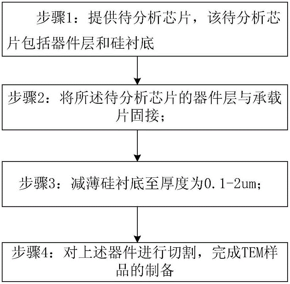
[0035] Such as image 3 Shown, the invention provides a kind of preparation method of TEM sample, comprising:
[0036] Step 1: If Figure 4 As shown, a chip to be analyzed 100 is provided. It should be noted that the chip to be analyzed 100 is a conventional product in the prior art, and does not require staff to spend time on special research, and the cost is low. Further, the chip to be analyzed 100 includes a device layer 110 and a silicon substrate 120 , and the size (length×width) of the chip to ...
PUM
| Property | Measurement | Unit |
|---|---|---|
| Thickness | aaaaa | aaaaa |
Abstract
Description
Claims
Application Information