Image detection method of printed circuit board

A technology for image detection and printed substrates, which is applied in the direction of optical testing for flaws/defects, can solve problems such as misjudgment, and achieve the effect of improving detection accuracy and reliability

Active Publication Date: 2018-03-09
SYNPOWER
View PDF4 Cites 0 Cited by
  • Summary
  • Abstract
  • Description
  • Claims
  • Application Information

AI Technical Summary

Problems solved by technology

[0004] The main purpose of the present invention is to solve the problem of misjudgment caused by the traditional use of optical images to detect printed circuit boards

Method used


Image

  • Image detection method of printed circuit board
  • Image detection method of printed circuit board
  • Image detection method of printed circuit board

Examples


Embodiment Construction

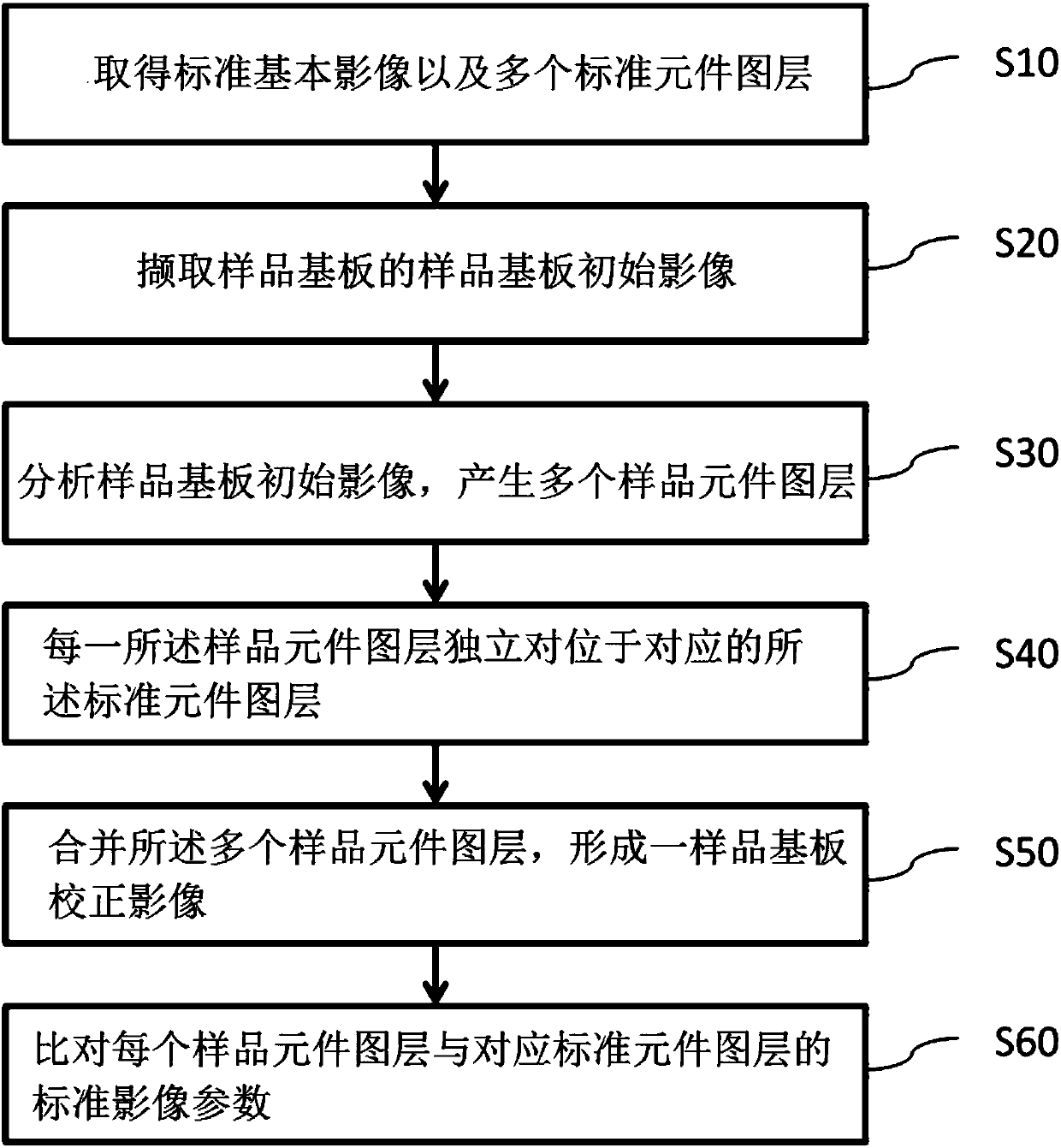
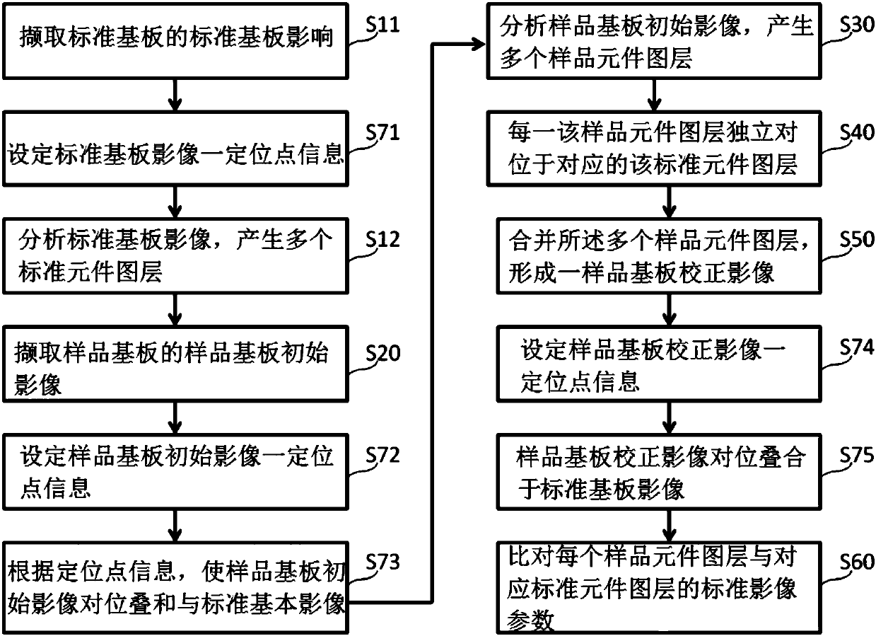
[0032] Relevant detailed description and technical content of the present invention, now just explain as follows with respect to matching drawing:

[0033] see figure 1 , which is a schematic flow diagram of the main steps of an embodiment of the image detection method for printed substrates of the present invention, as shown in the figure: the image detection method for printed substrates of the present invention includes the following steps:

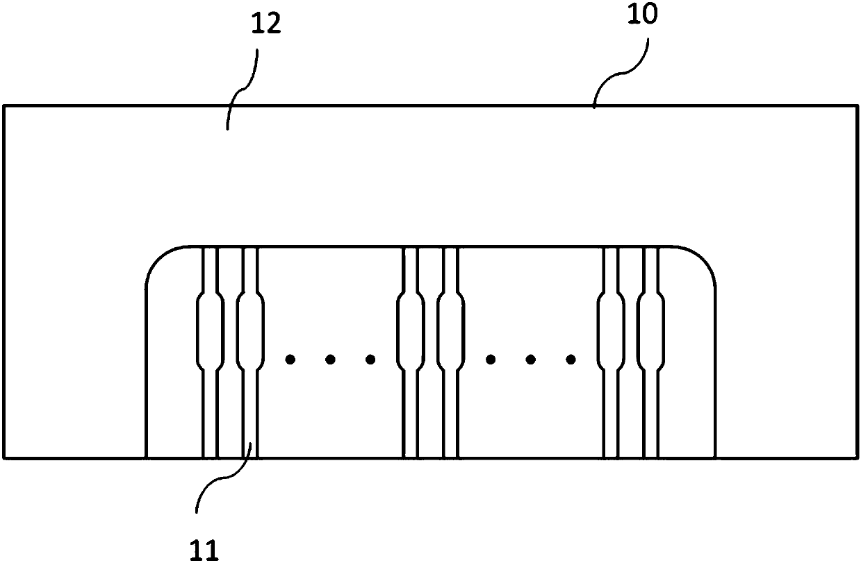
[0034] a) Obtaining a standard substrate image with multiple component areas and multiple standard component layers corresponding to each of the standard component areas, the standard component layer including a position information and at least one standard image parameter (step S10); wherein , the standard component area is the metal circuit layer area, the protective layer area, the through hole area or the solder mask area; the standard image parameter is the multi-primary color element value, and the multi-primary color element va...


PUM


Abstract

The invention discloses an image detection method of a printed substrate, comprising the following steps: capturing an initial sample substrate image of a sample substrate, the sample substrate initial image including a plurality of sample component regions; analyzing the sample substrate initial image to generate a corresponding A plurality of sample component layers of the plurality of sample component regions, and obtain a position information of the sample component layer and sample image parameters; each of the sample component layers independently corresponds to a standard component image located in the corresponding standard substrate image layer; combine the plurality of sample element layers to form a sample substrate correction image; and superimpose the sample substrate correction image and the standard substrate image, and compare the sample image parameters of each sample element layer with each The corresponding standard image parameters of the standard component layer.

Description

technical field [0001] The invention relates to an image detection method of a printed substrate, in particular to an image detection method of a printed substrate in which a corrected image is formed after each component layer is aligned independently and then detected. Background technique [0002] Printed circuit boards are currently widely used as necessary components of various electronic products, and their performance determines the quality of the electronic products. The manufacturing process of printed circuit boards is quite complex and precise, requiring a large number of machining, chemical etching, surface treatment and other process technologies to complete. In order to ensure the quality of finished printed circuit boards, an inspection process is added to the back-end process of manufacturing printed circuit boards. In addition to the inspection of electrical characteristics, the appearance inspection of printed circuit boards is carried out by manual visual...

Claims


Application Information

Patent Timeline
Patent Type & Authority Patents(China)
IPC IPC(8): G01N21/95
Inventor 林向如
Owner SYNPOWER
Why Eureka
Try Eureka