Apparatus and method for configuring data strobe signals in a memory device
A memory and signal technology, applied in the field of devices for configuring data strobe signals, can solve problems such as data transmission errors and delay deterioration
- Summary
- Abstract
- Description
- Claims
- Application Information
AI Technical Summary
Problems solved by technology
Method used
Image

Examples
Embodiment Construction
[0058] The following embodiments and figures will illustrate in more detail.
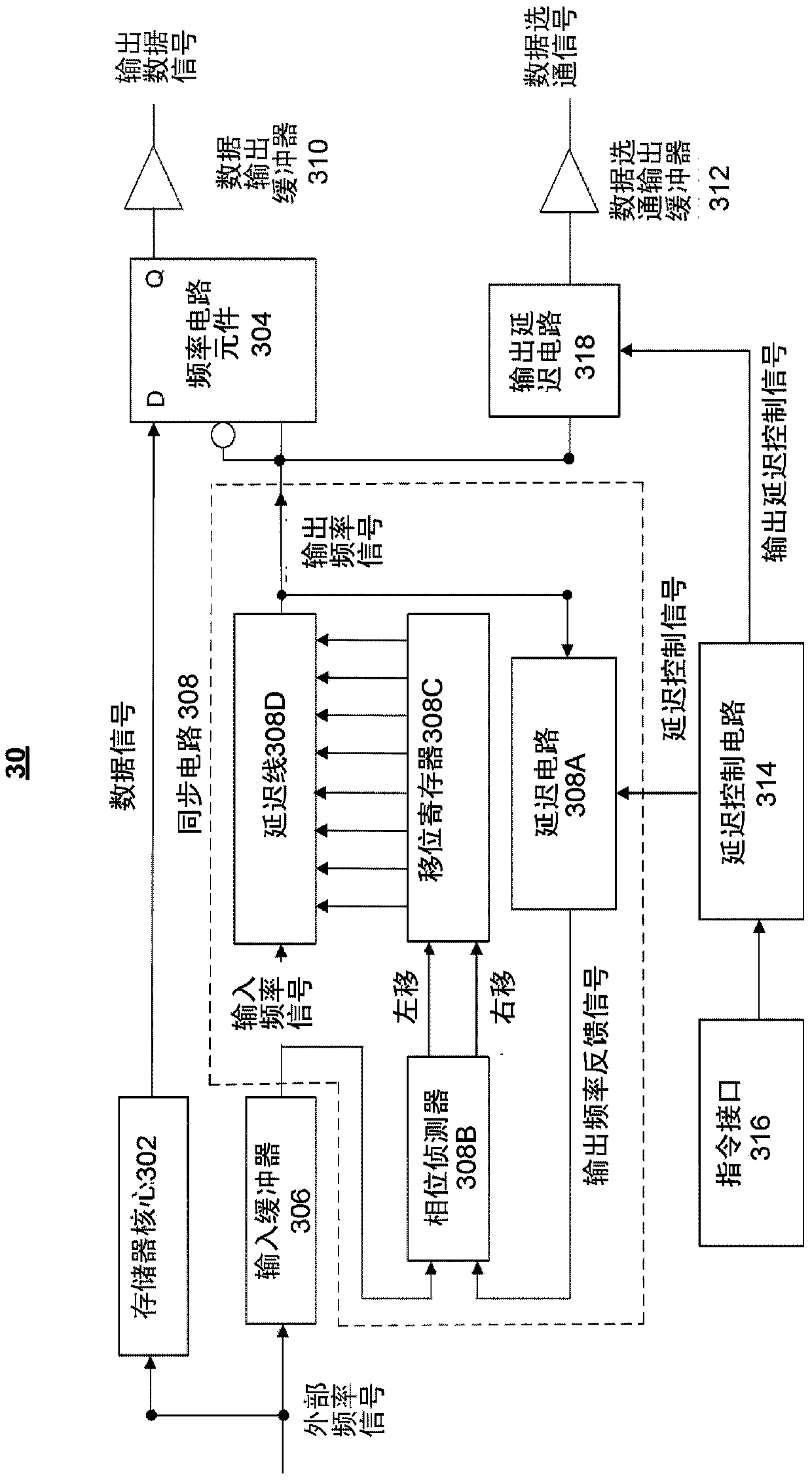
[0059] See image 3 , which is a schematic diagram of a non-volatile memory device 30 . The non-volatile memory device 30 includes a memory core 302 , a clock circuit element 304 , an input buffer 306 , a synchronization circuit 308 , a data output buffer 310 , a data strobe output buffer 312 , and a delay control circuit 314 .
[0060] The memory core 302 includes: a memory array, a logic control unit, a column address decoder, a row address decoder, and a sense amplifier. A memory array contains multiple memory cells arranged in rows and columns. Memory cells located in the same column are connected by word lines, and memory cells located in the same row are connected by bit lines. The sense amplifier is coupled to the bit line. The logic control unit is synchronized with an external frequency signal, or operates based on an internal oscillator. The logic control unit controls different memor...
PUM
 Abstract
Description
Claims
Application Information
 - R&D
- Intellectual Property
- Life Sciences
- Materials
- Tech Scout
- Unparalleled Data Quality
- Higher Quality Content
- 60% Fewer Hallucinations
Browse by: Latest US Patents, China's latest patents, Technical Efficacy Thesaurus, Application Domain, Technology Topic, Popular Technical Reports.
© 2025 PatSnap. All rights reserved.Legal|Privacy policy|Modern Slavery Act Transparency Statement|Sitemap|About US| Contact US: help@patsnap.com