Photoelectric detector assembly

A technology of photodetectors and components, applied in military and national economic fields, can solve the problems of photoresponsivity and photosensitive area limitation, cost increase, and inability to adapt to mass production, etc., to achieve the effect of improving optical power response and increasing production cost

Inactive Publication Date: 2015-12-16
INST OF SEMICONDUCTORS - CHINESE ACAD OF SCI
View PDF4 Cites 4 Cited by
  • Summary
  • Abstract
  • Description
  • Claims
  • Application Information

AI Technical Summary

Problems solved by technology

However, the photoresponsivity and photosensitive area are limited by the process conditions and process level. After reaching a certain level, it is difficult to continue to improve, and the cost is also greatly increased, which cannot meet the requirements of mass production.

Method used


Image

  • Photoelectric detector assembly
  • Photoelectric detector assembly

Examples


Embodiment Construction

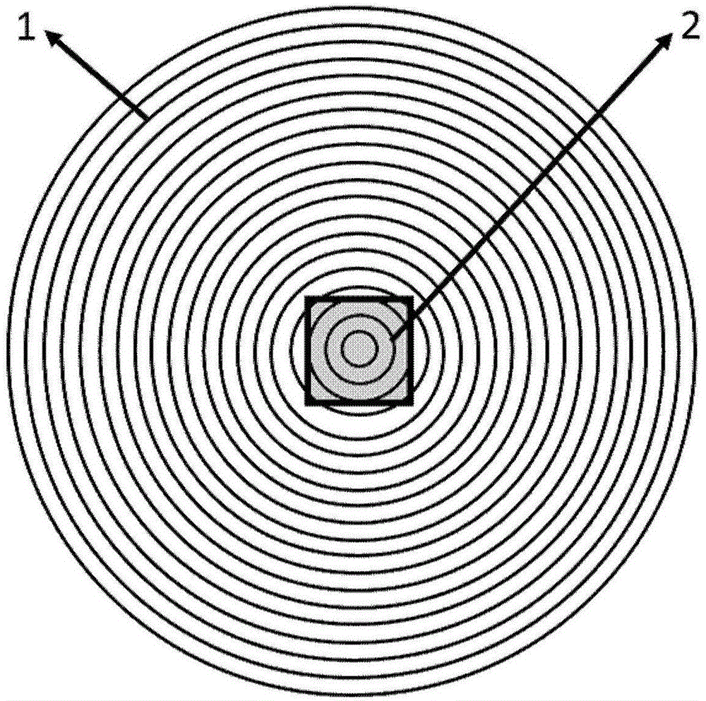
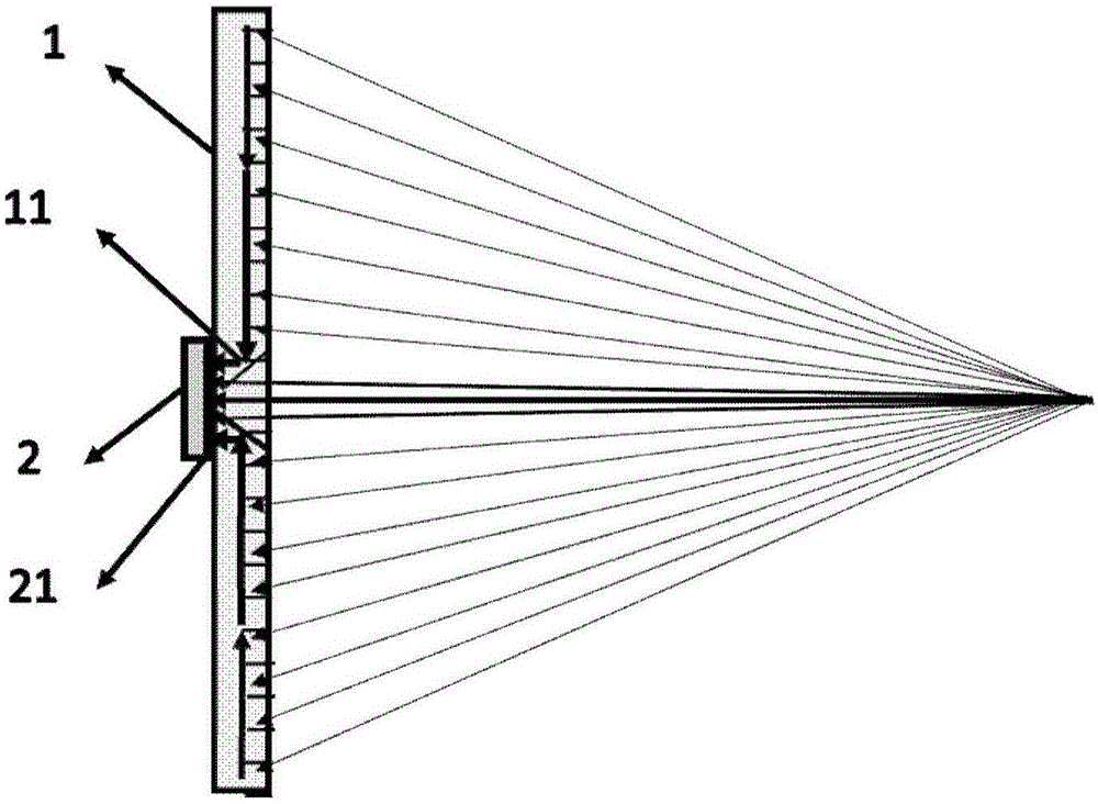
[0011] See figure 1 and figure 2 As shown, the present invention provides a photodetector assembly, which includes:

[0012] A waveguide grating 1, the shape of the waveguide grating 1 can be any shape according to the needs of use, which changes the optical power incident on its surface and the propagation direction of the optical signal through the diffraction and refraction effects of the grating, and collects and collects the optical power and the optical signal. Convergence, the material of the waveguide grating 1 is any one of silicon on the insulating layer, silicon-based silicon dioxide, silicon dioxide, glass, and polymer. The grating of the waveguide grating 1 is designed according to the requirements of use and passed The processing technology of electron beam direct writing, photolithography, plasma etching or electron beam exposure is completed. The waveguide grating 1 has a light exit hole 11 in the center. The grating is distributed from the inside to the outside...


PUM


Abstract

A photoelectric detector assembly comprises: a waveguide grating which is in arbitrary shape, changes propagation directions of optical power and optical signals incident on a surface of the waveguide grating through diffraction and refraction effects of the waveguide grating, and collects and gathers the optical power and the optical signals; and a semiconductor photoelectric detector arranged at a center position corresponding to a light outlet hole at one side of the waveguide grating, wherein one side of the semiconductor photoelectric detector opposite to the waveguide grating is a photosensitive surface used for converting the received optical power and the optical signals into electric signals. Through combination of the waveguide grating and the semiconductor photoelectric detector, the photoelectric detector assembly of the present invention can improve optical power response of the photoelectric detector and a detection area of the optical signals, and can greatly reduce production cost at the same time, thereby providing powerful guarantee for better and wider application of the photoelectric detector.

Description

Technical field [0001] The invention relates to various fields of military and national economy, and more specifically is a photodetector assembly. Background technique [0002] Due to the advantages of small size, light weight, fast response speed, and easy integration with other semiconductor devices, photodetectors are widely used in the fields of optical communications, signal processing, optical sensing systems, and optical measurement. In recent years, with the expansion of the application range of photodetectors, the market has put forward more and higher requirements on the index parameters and structural dimensions of photodetectors. For example, under certain special environments and conditions, the light energy to be measured The light signal is relatively weak. In order to receive as much light energy as possible and detect weak light signal changes, the goal can only be achieved by increasing the photoresponse of the detector or by increasing the photosensitive area ...

Claims


Application Information

Patent Timeline
Patent Type & Authority Applications(China)
IPC IPC(8): H01L31/0232H01L31/09
CPCH01L31/02325H01L31/09
Inventor 王欣刘宇祝宁华
Owner INST OF SEMICONDUCTORS - CHINESE ACAD OF SCI
Why Eureka
Try Eureka