Manufacturing method of array substrate and array substrate

A technology of an array substrate and a manufacturing method, which is applied in the display field, can solve problems such as surface defects of polysilicon layers, influence TFT characteristics, etc., and achieve the effect of improving loss

Active Publication Date: 2015-12-23
WUHAN CHINA STAR OPTOELECTRONICS TECH CO LTD
View PDF3 Cites 10 Cited by
  • Summary
  • Abstract
  • Description
  • Claims
  • Application Information

AI Technical Summary

Problems solved by technology

[0004] The object of the present invention is to provide a manufacturing method of an array substrate and an array substrate, aiming at solving the ion implantation process e...

Method used


Image

  • Manufacturing method of array substrate and array substrate
  • Manufacturing method of array substrate and array substrate
  • Manufacturing method of array substrate and array substrate

Examples


Embodiment 1

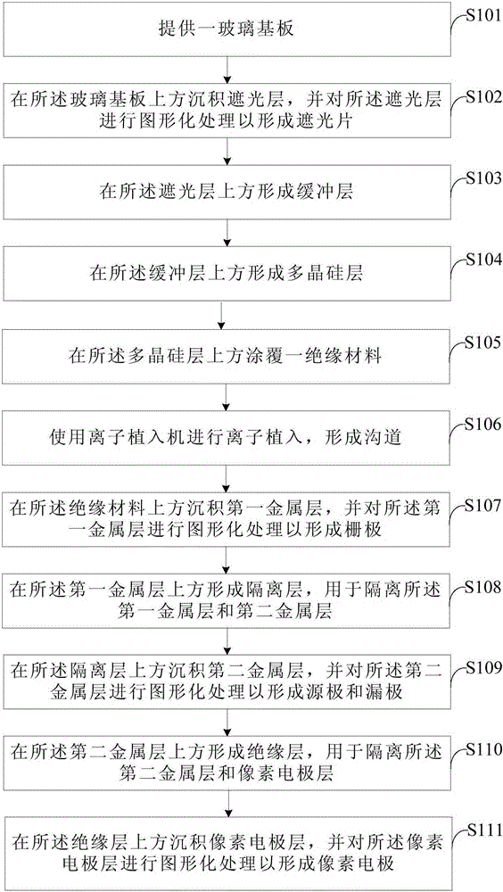
[0068] see figure 2 , is the implementation process of the method for manufacturing an array substrate provided in Embodiment 1 of the present invention, which mainly includes the following steps:

[0069] In step S201, a glass substrate is provided;

[0070] In step S202, a light-shielding layer is deposited on the glass substrate, and the light-shielding layer is patterned to form a light-shielding sheet;

[0071]In step S203, a buffer layer is formed on the light shielding layer;

[0072] In the embodiment of the present invention, a silicon nitride layer and a silicon oxide layer are sequentially formed on the light shielding layer, so as to obtain a buffer layer.

[0073] In step S204, forming a polysilicon layer on the buffer layer;

[0074] In an embodiment of the present invention, an amorphous silicon layer is formed on the buffer layer;

[0075] An excimer laser annealing operation is performed on the amorphous silicon layer to form a polycrystalline silicon lay...

Embodiment 2

[0088] see image 3 , is the implementation process of the method for manufacturing an array substrate provided in Embodiment 2 of the present invention, which mainly includes the following steps:

[0089] In step S301, a glass substrate is provided;

[0090] In step S302, a light-shielding layer is deposited on the glass substrate, and the light-shielding layer is patterned to form a light-shielding sheet;

[0091] In step S303, a buffer layer is formed on the light shielding layer;

[0092] In the embodiment of the present invention, a silicon nitride layer and a silicon oxide layer are sequentially formed on the light shielding layer, so as to obtain a buffer layer.

[0093] In step S304, forming a polysilicon layer on the buffer layer;

[0094] In an embodiment of the present invention, an amorphous silicon layer is formed on the buffer layer;

[0095] An excimer laser annealing operation is performed on the amorphous silicon layer to form a polycrystalline silicon lay...

Embodiment 3

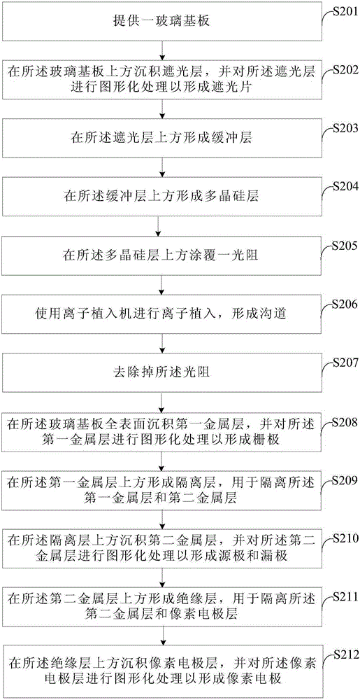
[0107] see Figure 4 , is the implementation process of the method for manufacturing an array substrate provided in Embodiment 3 of the present invention, which mainly includes the following steps:

[0108] In step S401, a glass substrate is provided;

[0109] In step S402, a light-shielding layer is deposited on the glass substrate, and the light-shielding layer is patterned to form a light-shielding sheet;

[0110] In step S403, a buffer layer is formed on the light shielding layer;

[0111] In the embodiment of the present invention, a silicon nitride layer and a silicon oxide layer are sequentially formed on the light shielding layer, so as to obtain a buffer layer.

[0112] In step S404, forming a polysilicon layer on the buffer layer;

[0113] In an embodiment of the present invention, an amorphous silicon layer is formed on the buffer layer;

[0114] An excimer laser annealing operation is performed on the amorphous silicon layer to form a polycrystalline silicon la...


PUM


Abstract

The present invention discloses a manufacturing method of an array substrate. The method comprises the steps of forming a shading layer, a buffer layer, a polycrystalline silicon layer, an insulating material, a first metal layer, an isolation layer, a second metal layer, an insulating layer and a pixel electrode layer orderly above a glass substrate; after the polycrystalline silicon layer is formed, firstly coating the insulating material above the polycrystalline silicon layer; and then using an ion Implanter to carry out the ion implantation above the insulating material, thereby forming a channel. Therefore, the problems that the ions are implanted on the polycrystalline silicon layer directly during the ion implantation process, thereby causing the surface defect of the polycrystalline silicon layer and influencing the TFT characteristic, are avoided effectively. According to the present invention, the surface loss of the polycrystalline silicon layer during the ion implantation process is improved effectively.

Description

【Technical field】 [0001] The present invention relates to the field of display technology, in particular to a method for manufacturing an array substrate and the array substrate. 【Background technique】 [0002] In the LTPS (Low Temperature Polysilicon) process, in order to fabricate the NMOS or PMOS channel layer, ion implantation is required. However, the ion implantation process in the prior art directly implants ions on the polysilicon layer, which easily causes surface defects of the polysilicon layer and affects the characteristics of the TFT. [0003] Therefore, it is necessary to propose a new technical solution to solve the above-mentioned technical problem of the loss of the polysilicon layer during ion implantation. 【Content of invention】 [0004] The purpose of the present invention is to provide a method for manufacturing an array substrate and an array substrate, aiming to solve the problem that the ion implantation process existing in the prior art is to dir...

Claims


Application Information

Patent Timeline
IPC IPC(8): H01L21/77H01L21/265H01L27/12
CPCH01L21/26506H01L21/77H01L27/1214H01L27/127H01L2021/775
Inventor 刘小花
Owner WUHAN CHINA STAR OPTOELECTRONICS TECH CO LTD
Why Eureka
Try Eureka