
Piezoelectric-triboelectric combined MEMS wideband-energy harvester and preparation method thereof

An energy harvester and piezoelectric energy technology, applied in the field of micro energy, can solve the problems of narrow frequency band and low output power, and achieve the effect of improving output performance, improving output performance and wide application prospects

Inactive Publication Date: 2015-12-23
NANCHANG INST OF TECH
View PDF6 Cites 13 Cited by
  • Summary
  • Abstract
  • Description
  • Claims
  • Application Information

AI Technical Summary

Problems solved by technology

[0005] One of the purposes of the present invention is to provide a piezoelectric-triboelectric composite MEMS broadband energy harvester and its preparation method to solve the defects of the prior art, so that the transducer element can obtain greater output power in a low-frequency vibration environment , to solve the problems of low output power and narrow frequency band of traditional MEMS piezoelectric energy harvesters

Method used


Image

  • Piezoelectric-triboelectric combined MEMS wideband-energy harvester and preparation method thereof
  • Piezoelectric-triboelectric combined MEMS wideband-energy harvester and preparation method thereof
  • Piezoelectric-triboelectric combined MEMS wideband-energy harvester and preparation method thereof

Examples


preparation example Construction

[0063] The present invention also provides a method for preparing a piezoelectric-triboelectric composite MEMS broadband energy harvester, comprising the following steps:

[0064] S1: Using bonding and thinning techniques to prepare a piezoelectric thick film layer on a silicon wafer, and fabricate a piezoelectric thick film electrode layer (5) on the surface of the piezoelectric thick film (3);

[0065] The silicon wafer refers to an SOI silicon wafer whose upper and lower surfaces are polished on both sides and a layer of silicon dioxide is thermally oxidized on the surface.

[0066] The step of preparing a piezoelectric thick film layer by bonding and thinning technology, specifically includes: combining the single-sided polished piezoelectric body with the silicon wafer through epoxy bonding technology, or combining the polished surface of the piezoelectric body with the silicon wafer After a layer of electrode layer is deposited on the surface, the piezoelectric material ...

Embodiment 1

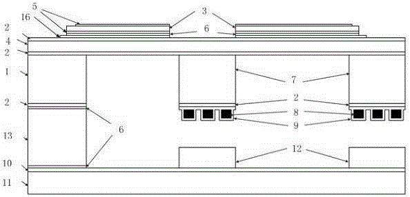
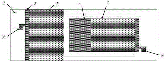
[0082] Such as figure 1 As shown, the piezoelectric-triboelectric composite MEMS energy harvester in this embodiment includes the main structure of the piezoelectric energy harvester, a blocking block and a gasket;

[0083] The main structure of the piezoelectric energy harvester includes: a silicon fixed base, 2 silicon-based piezoelectric cantilever beams and 2 mass blocks;

[0084] The silicon fixed base includes: a silicon wafer (1) and silicon dioxide layers (2) on both sides thereof;

[0085] The silicon-based piezoelectric cantilever beam on the piezoelectric main structure includes: a silicon cantilever beam support layer and a piezoelectric thick film layer attached to the silicon cantilever beam support layer; the silicon cantilever beam support layer includes a second silicon layer (4), a The silicon dioxide layer (2) on the upper and lower surfaces of the second silicon layer (4) and the supporting layer electrode layer (16) on the silicon dioxide layer (2) on the...

Embodiment 2

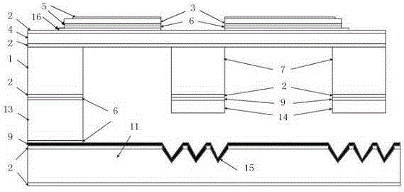
[0114] Such as image 3 As shown, a piezoelectric-triboelectric composite MEMS energy harvester provided in this embodiment includes: a main structure of the piezoelectric energy harvester, a blocking block and a gasket.

[0115] The main structure of the piezoelectric energy harvester includes: a silicon fixed base, 2 silicon-based piezoelectric cantilever beams and 2 mass blocks;

[0116] The silicon fixing base comprises: a silicon wafer (1) and silicon dioxide layers (2) on both sides thereof;

[0117] The silicon-based piezoelectric cantilever beam on the piezoelectric main structure includes: a silicon cantilever beam support layer and a piezoelectric thick film layer attached to the silicon cantilever beam support layer; the silicon cantilever beam support layer includes a second silicon layer (4), a The silicon dioxide layer (2) on the upper and lower surfaces of the second silicon layer (4) and the supporting layer electrode layer (16) on the silicon dioxide layer (2...


PUM

PropertyMeasurementUnit
thicknessaaaaaaaaaa
thicknessaaaaaaaaaa
thicknessaaaaaaaaaa

Abstract

The invention discloses a piezoelectric-triboelectric combined MEMS wideband-energy harvester and a preparation method thereof. The harvester comprises a main structure of a piezoelectric energy harvester, a stop block and a gasket, wherein the main structure of the piezoelectric energy harvester comprises a fixed silicon base, silicon-based piezoelectric cantilever beams and masses; the fixed silicon base comprises a silicon layer and silicon dioxide layers at two sides of the silicon layer; the silicon-based piezoelectric cantilever beam comprises a silicon cantilever beam supporting layer and a piezoelectric thick film layer arranged on the silicon cantilever beam supporting layer; the silicon cantilever beam supporting layer comprises a silicon layer, silicon dioxide layers and a supporting layer electrode layer; the piezoelectric thick film layer comprises a piezoelectric thick film and a piezoelectric thick film electrode layer arranged on the surface of the piezoelectric thick film; each mass comprises an integrated silicon mass and a frictional layer arranged on the surface of the integrated silicon mass; the stop block comprises a frictional layer base, an electrode layer and a frictional layer; and the gasket is located between the fixed silicon base and the stop block. By using the piezoelectric-triboelectric combined MEMS wideband-energy harvester, a transduction element can obtain relatively high output power in a low-frequency vibration environment, so that the problems of low output power, narrow frequency band and the like of the traditional MEMS piezoelectric energy harvester are solved.

Description

technical field [0001] The invention belongs to the field of micro-energy technology, and in particular relates to a piezoelectric-triboelectric composite MEMS broadband energy collector and a preparation method thereof. Background technique [0002] Wireless Sensor Network (Wireless Sensor Network, referred to as WSN) is a network composed of low-cost, dense, randomly distributed tiny nodes integrated with sensors, data processing units and short-range wireless communication modules through self-organization. With the help of various types of sensors built into the nodes, it senses, collects and monitors the surrounding environmental signals, and finally realizes all-round monitoring and control of the physical world we live in. Low-power, small-sized wireless sensor nodes are fundamental components of WSNs, usually powered by common chemical batteries. However, considering that the batteries carried by these sensors have a limited lifespan and a large number, and may be i...

Claims


Application Information

Patent Timeline
Patent Type & Authority Applications(China)
IPC IPC(8): H02N1/04H02N2/18B81C3/00
CPCB81C3/001H02N1/04H02N2/183H02N2/22
Inventor 唐刚邬文静胡敏李志彪徐斌闫肖肖邓小珍徐兵侯诚
Owner NANCHANG INST OF TECH
Learn More