Reset device

A reset device and thin-film transistor technology, applied in the direction of instruments, static indicators, etc., can solve the problems of affecting the discharge of drive circuit units, reset signal Reset distortion, and affecting the output characteristics of thin-film transistors, so as to ensure normal display and stable reset signal. Effect

Active Publication Date: 2015-12-30
BOE TECH GRP CO LTD +1
View PDF5 Cites 4 Cited by
  • Summary
  • Abstract
  • Description
  • Claims
  • Application Information

AI Technical Summary

Problems solved by technology

[0006] exist figure 1 In the shown reset circuit, for the thin film transistor M1, since the clock signal CLKB continuously provides a higher voltage to the gate of the thin film transistor M1, the threshold voltage of the thin film transistor M1 will drift greatly, while the thin film transistor The drift of the threshold voltage will affect the output characteristics of thin film transistors
In this case, after the reset circuit works for a long time, the reset signal Reset provided may be distorted, thereby affecting the discharge of the driving circuit unit and causing abnormal display of the liquid crystal device, etc.

Method used


Image

  • Reset device
  • Reset device
  • Reset device

Examples


Embodiment Construction

[0028] In order to make the purpose, technical solutions and advantages of the embodiments of the present invention clearer, the technical solutions of the embodiments of the present invention will be clearly and completely described below in conjunction with the accompanying drawings. Apparently, the described embodiments are some, not all, embodiments of the present invention. Based on the described embodiments of the present invention, all other embodiments obtained by those skilled in the art without creative efforts also fall within the protection scope of the present invention.

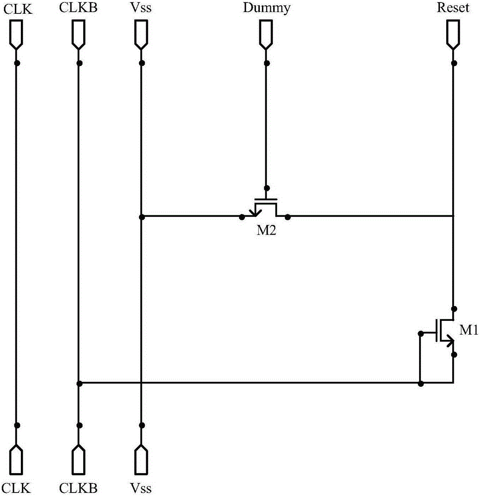
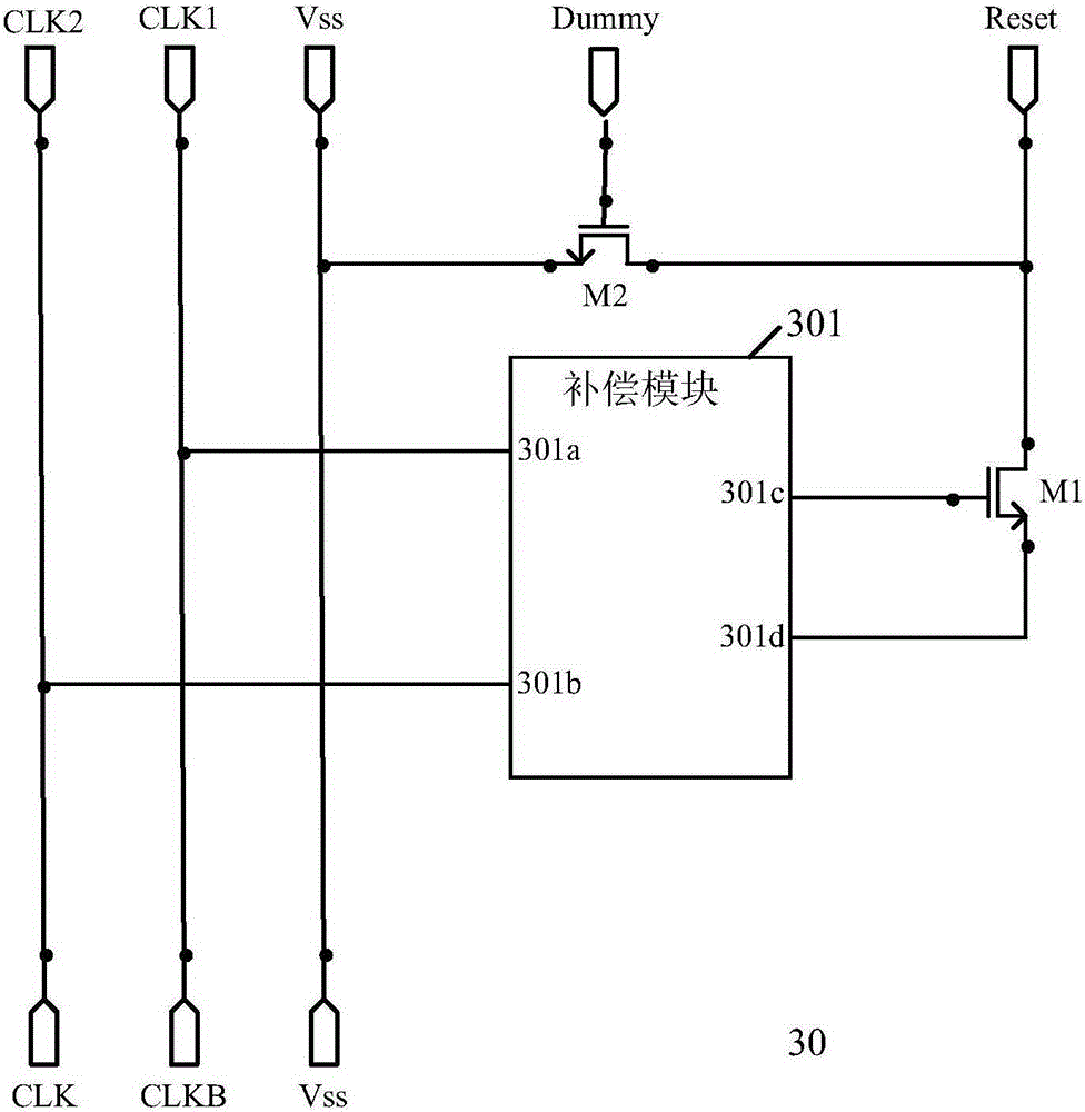
[0029] image 3 A schematic diagram of a reset device 30 according to an embodiment of the invention is shown. The reset device 30 of this embodiment can be applied to a GOA circuit to provide a reset signal to the driving circuit unit. Such as image 3 As shown, the reset device 30 may include a first thin film transistor M1 , a second thin film transistor M2 and a compensation module 301 . ...


PUM


Abstract

The embodiment of the invention provides a reset device, an array substrate grid electrode driver and a liquid crystal device. The reset device comprises a first thin film transistor, a second thin film transistor and a compensation module. The first thin film transistor is used for outputting reset signals from a drain electrode. A grid electrode of the second thin film transistor is used for receiving output signals from the grid electrode driver, a drain electrode of the second thin film transistor is connected with the drain electrode of the first thin film transistor, and a source electrode of the second thin film transistor is grounded. The compensation module is used for compensating for threshold voltage of the first thin film transistor and is provided with a first input end, a second input end, a first output end and a second output end. The first input end receives first clock signals, the second input end receives second cloth signals, the first output end is connected with a grid electrode of the first thin film transistor, and the second output end is connected with a source electrode of the first thin film transistor. The first clock signals and the second clock signals have the difference of a half cycle, and the lasting time of a high level is shorter than that of a lower level.

Description

technical field [0001] The present invention relates to an array substrate gate drive (GateOnArray, GOA for short) technology, in particular, to a reset device used in a GOA circuit. Background technique [0002] In current liquid crystal devices, it is becoming more and more common to use a GOA circuit as a gate driving circuit. Generally, a GOA circuit may include one or more driving circuit units for providing gate signals and a reset circuit. The reset circuit provides a reset signal to the driving circuit unit, so that the driving circuit unit is reset in response to the reset signal, thereby realizing driving and refreshing of different rows. In addition, since the driving circuit unit is reset, the driving circuit unit is discharged, so the noise signal in the GOA circuit can be eliminated in real time. [0003] At present, the reset circuit can provide a reset signal based on a frame start signal (ie, an initial scan signal provided by an external driving circuit u...

Claims


Application Information

Patent Timeline
Patent Type & Authority Applications(China)
IPC IPC(8): G09G3/36
Inventor 钱先锐
Owner BOE TECH GRP CO LTD
Why Eureka
Try Eureka