
Display device

A technology of display equipment and thin film transistors, which is applied to electrical components, electrical solid devices, circuits, etc., and can solve the problems of weakening the intensity of short-wavelength light shading layers, etc.

Inactive Publication Date: 2016-01-06
INNOLUX CORP
View PDF7 Cites 22 Cited by
  • Summary
  • Abstract
  • Description
  • Claims
  • Application Information

AI Technical Summary

Problems solved by technology

[0007] Accordingly, the present invention utilizes the light-shielding layer to absorb short-wavelength light (such as irradiating ultraviolet light, purple light or blue light in the process, or ultraviolet light, purple light or blue light from the external environment), and weakens the penetration of short-wavelength light into the light-shielding layer. Intensity, in this way, can effectively reduce short-wavelength light from contacting the active layer channel of the thin film transistor unit, thereby reducing the electrical offset of the thin film transistor unit, and improving the light leakage phenomenon or displacement of the display device in the dark state operation Registers, data multiplexers, and other driving circuits cannot operate normally. Therefore, the display device of the present invention can provide more stable and higher-quality display effects

Method used


Image

  • Display device
  • Display device
  • Display device

Examples


Embodiment 1

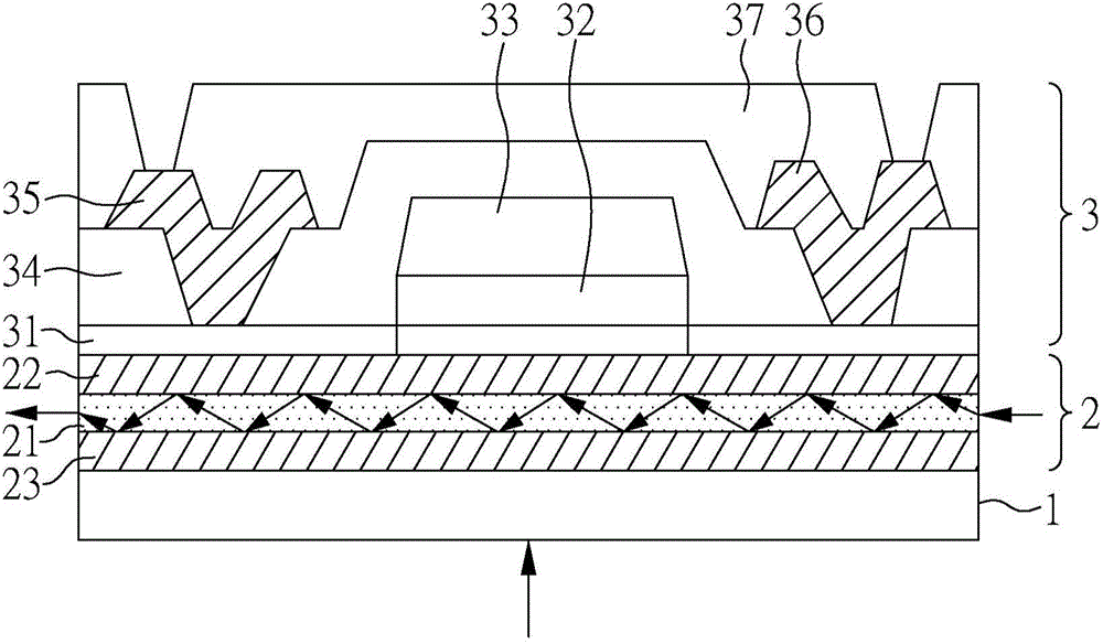
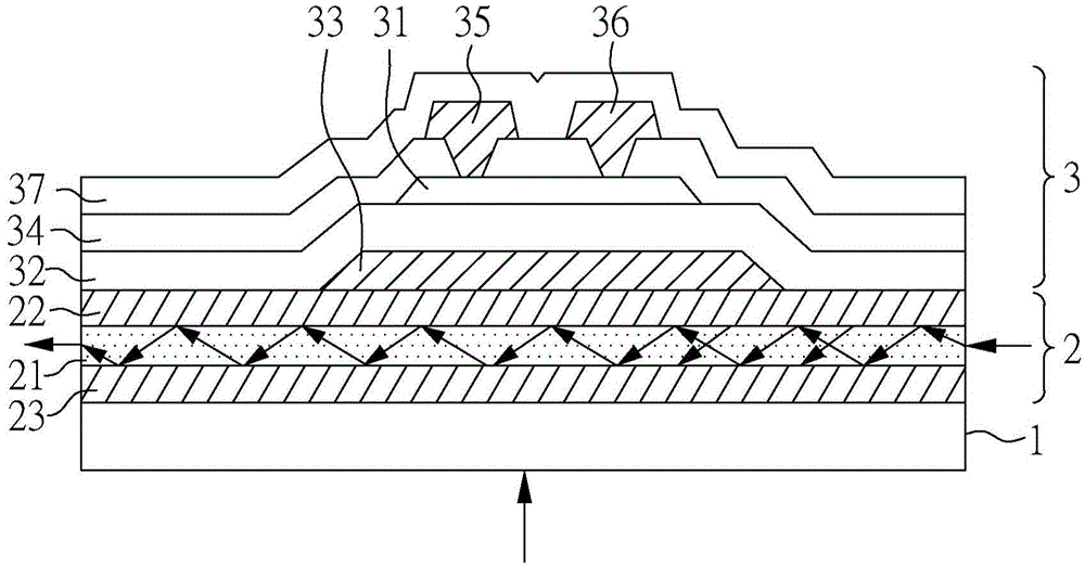
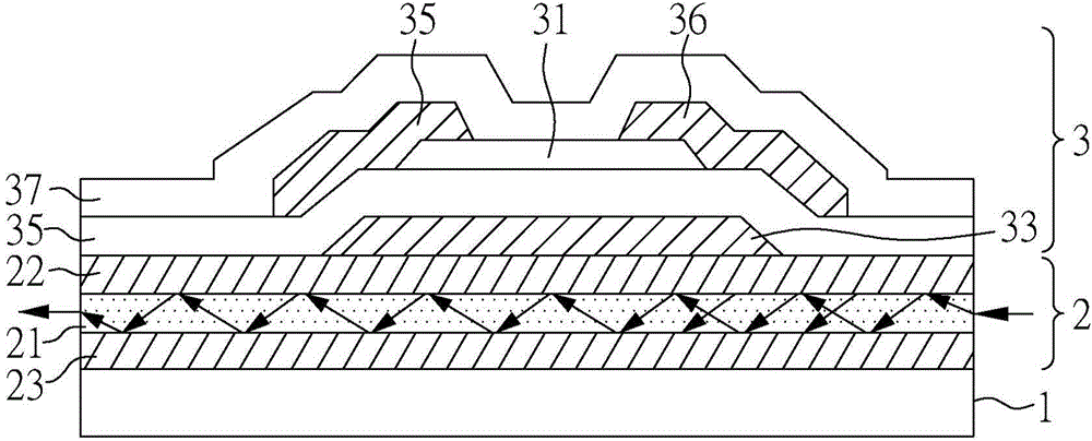
[0031] Please refer to figure 1 , The display device of the present invention includes: a substrate 1; a thin film transistor unit 3, disposed on the substrate 1, and the thin film transistor unit 3 includes: a semiconductor layer 31, an insulating layer 32, a grid 33, a first A protective layer 34, a source 35, a drain 36, and a second protective layer 37; and a light shielding unit 2, disposed between the substrate 1 and the TFT unit 3, and the light shielding unit 2 includes: A light-shielding layer 21, a first buffer layer 22, and optionally a second buffer layer 23, the first buffer layer 22 is arranged between the light-shielding layer 21 and the thin film transistor unit 3, the second buffer layer 23 is disposed between the light shielding layer 21 and the substrate 1 .

[0032] In this embodiment, the thin film transistor unit 3 can be manufactured using an existing thin film transistor process, so details are not repeated here; figure 1 Shown is a top gate TFT unit,...

Embodiment 2

[0041] Please refer to Image 6 The display device, except for the light-shielding layer 21, the rest are all with figure 2 The same, the same part will not be repeated, and the content of Embodiment 1 can be applied here. In this embodiment, the display device provided is a bottom emitting organic light emitting diode device (bottom emitting OLED), and the organic light emitting diode 8 disposed on the thin film transistor unit 3 includes a light emitting region 81; According to the procedure, the light-shielding layer 21 has an opening 211 corresponding to the light-emitting area 81 . Here, the size and shape of the opening 211 are not limited, and can be easily adjusted by those skilled in the art according to actual conditions or needs. Therefore, since the light-shielding layer 21 does not exist in the portion corresponding to the light-emitting area 81 , when the display device emits light downward, the light will not be blocked by the light-shielding layer 21 to affe...


PUM

PropertyMeasurementUnit
Thicknessaaaaaaaaaa

Abstract

The invention relates to a display device. The display device includes: a substrate; a thin film transistor unit positioned on the substrate and including a gate, an insulation layer, a semiconductor layer, a source and a drain; a shading unit positioned between the substrate and the thin film transistor unit and including a shading layer and a first buffer layer, wherein the first buffer layer is arranged between the shading layer and the thin film transistor unit; wherein the penetration rate of light through the shading layer is 0 to 15%, and the wavelength range of the light is between 200 nm and 510 nm.

Description

technical field [0001] The invention relates to a display device, in particular to a display device which improves the stability of a thin film transistor unit. Background technique [0002] With the continuous advancement of display technology, users have higher and higher requirements for electronic products. All devices are developing towards small size, thin thickness, and light weight. Therefore, the current mainstream display devices on the market have changed from the previous cathode ray Tubes are developed into liquid crystal display devices (LCD) or organic light emitting diode devices (OLED). [0003] In LCD or OLED, since the energy gap of the active layer material of the thin film transistor unit (TFT) is generally similar to ultraviolet light (UV) and blue light, TFT is very sensitive to ultraviolet light, purple light and blue light. Or under blue light irradiation (such as ultraviolet light, purple light or blue light in the process, or ultraviolet light, pu...

Claims


Application Information

Patent Timeline
IPC IPC(8): H01L23/552H01L27/32
Inventor 周政旭沈羲和张志雄
Owner INNOLUX CORP
Learn More