Method for improving copper-free hole metallization

A technology without copper holes and copper layers, which is applied in the direction of electrical components, printed circuits, printed circuit manufacturing, etc., can solve the problems that affect the appearance and yield of printed circuit boards, cannot be cleaned, and are easy to gold, etc., to save palladium removal Effects of potion, improvement of cloaking problem, and improvement of appearance

Inactive Publication Date: 2016-01-06
SHENZHEN SUNTAK MULTILAYER PCB
View PDF3 Cites 1 Cited by
  • Summary
  • Abstract
  • Description
  • Claims
  • Application Information

AI Technical Summary

Problems solved by technology

[0004] For this reason, the technical problem to be solved by the present invention is that the deposited copper in the copper-free holes in the prior art cannot be removed after etching and cleaning with palladium-removing liquid medicine, which leads to easy gold deposits in the copper-free holes, which affects the appearance and yield of printed circuit boards. , thus proposing a method to improve gold-on-porous copper

Method used


Image

  • Method for improving copper-free hole metallization

Examples


Embodiment

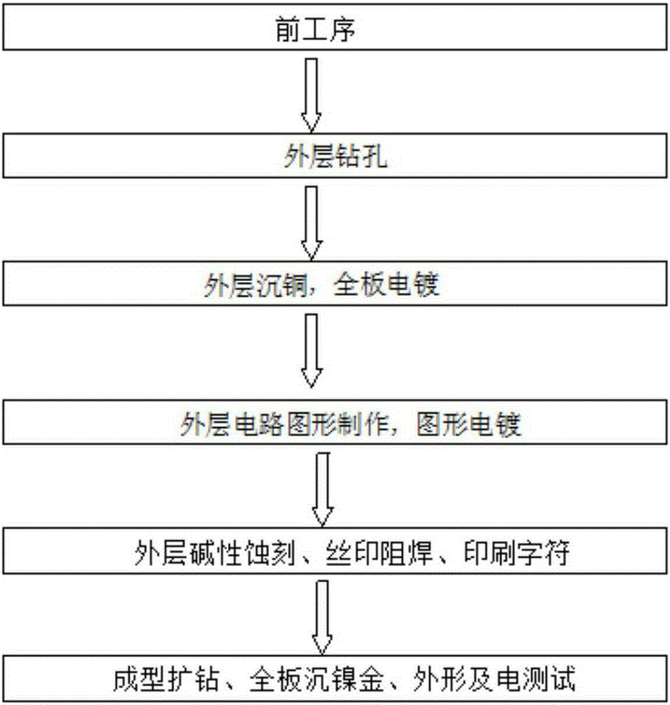
[0030] This embodiment provides a method for improving gold on copper-free holes, which includes the following steps:

[0031] S1. Pre-process: Carry out cutting of the circuit board substrate: cut out the core board according to the size of the imposition; inner layer graphic printing: complete the line exposure of the inner layer core board with a 6-grid exposure ruler, and have different thicknesses of the inner layer copper after development Etching out the circuit pattern of the inner core board; Lamination of the inner and outer layers: select appropriate lamination conditions according to the glass transition temperature of the sheet to carry out lamination of the inner core board and the outer copper foil;

[0032] S2. Drilling the outer layer. According to the board thickness, use the drilling data and use the drill to drill through holes and copper-free holes on the outer layer of the printed circuit board. The size of the copper-free hole requires that the diameter o...


PUM


Abstract

The invention discloses a method for improving copper-free hole metallization, comprising the steps as follows: S1, a front process; S2, outer-layer hole drilling: a copper-free hole is drilled by a drill bit in the outer layer of a printed circuit board; S3, outer-layer copper deposition, hole metallization and full-board electroplating; S4, outer-layer pattern making and pattern electroplating; S5, outer-layer alkaline etching: the made line and copper in the copper-free hole are etched; and S6, molding and counter-boring: the residual copper processed in step S5 in the copper-free hole is removed, and the hole aperture of the copper-free hole is made to reach a default value. By adopting the method, the copper layer in the copper-free hole can be removed completely, subsequent gold plating in the copper-free hole is avoided, the appearance of the printed circuit board is improved, the problem that the whole circuit board is scraped due to metallization in the copper-free hole is prevented, the product yield is increased, no palladium removal is needed after outer-layer alkaline etching, and the production cost is reduced.

Description

technical field [0001] The invention belongs to the technical field of printed circuit board production, and relates to a method for improving a printed circuit board, in particular to a method for improving gold on non-porous copper. Background technique [0002] The printed circuit board (Printed Circuit Board, referred to as PCB), realizes the electrical connection between the component pins through the printed wires, pads and metallized vias on the printed board. Since the conductive graphics on the printed board (such as component pin pads, printed wiring, vias, etc.) circuit board. Through a certain process, a layer of copper film with good conductivity is covered on a substrate with high insulation performance, which constitutes the material necessary for the production of printed circuit boards - copper clad laminates. According to the circuit requirements, the conductive pattern is etched on the copper clad laminate, and the mounting holes for the component pins, ...

Claims


Application Information

Patent Timeline
Patent Type & Authority Applications(China)
IPC IPC(8): H05K3/00
CPCH05K3/0047H05K2201/10401
Inventor 王佐朱拓周文涛
Owner SHENZHEN SUNTAK MULTILAYER PCB
Why Eureka
Try Eureka