Physical system of ultra-thin chip-level atomic clock

A chip atomic clock and physical system technology, which is applied in the field of chip atomic clock physical systems, can solve the problems of restricting the popularization and use of chip-level atomic clocks, high production costs, and responsible structure, and achieve the effect of simple structure, low cost, and elimination of outgassing

Active Publication Date: 2016-01-13
CHENGDUSCEON ELECTRONICS
View PDF7 Cites 6 Cited by
  • Summary
  • Abstract
  • Description
  • Claims
  • Application Information

AI Technical Summary

Problems solved by technology

Chip-level atomic clocks are a kind of atomic clocks, which are widely used in various fields. However, in the prior art, chip-level atomic clocks mainly

Method used


Image

  • Physical system of ultra-thin chip-level atomic clock
  • Physical system of ultra-thin chip-level atomic clock
  • Physical system of ultra-thin chip-level atomic clock

Examples


Embodiment

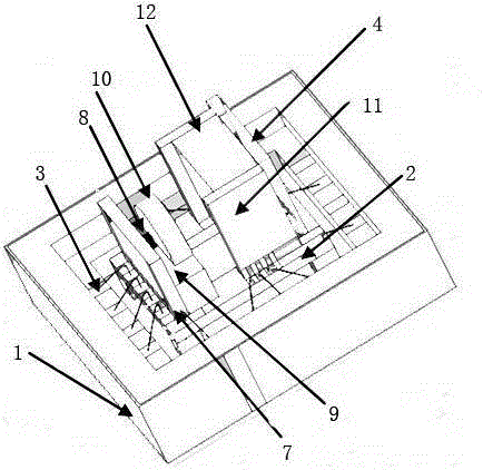
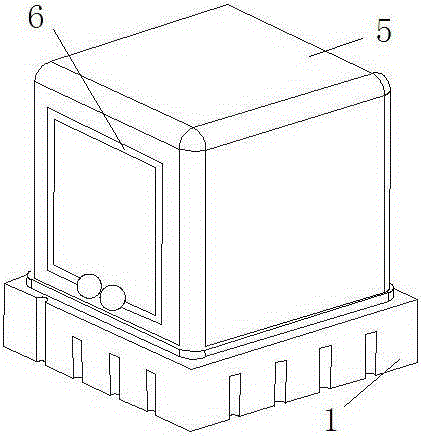
[0030] like Figure 1-4 As shown, this embodiment provides an ultra-thin chip atomic clock physics system, the chip atomic clock physics system is composed of an LCC base 1 and a ceramic cap 5 to form a sealed structure, and other components are arranged in the sealed structure. Vacuum seal welding is used between the LCC base and the ceramic cap, and the specific process is as follows: heat the metal welding consumables to 250°C for 2 hours, and then the ceramic cap and the LCC base of the physical system can be vacuum sealed and welded. The role is to realize the vacuum packaging of the physical system and reduce power consumption.

[0031] In order to simplify the C field structure of the present invention, in this embodiment, two metal traces 6 are arranged symmetrically on the outer wall of the ceramic cap 5, and the two metal traces made on the ceramic cap can be equivalent to two symmetrically placed Helm Holtz coils will generate a constant magnetic field with better ...


PUM


Abstract

The invention discloses a physical system of an ultra-thin chip-level atomic clock for the purpose of solving the problem of a conventional chip-level atomic clock is high in cost and energy consumption in structure duplication. The physical system of the ultra-thin chip-level atomic clock comprises an LCC base, a physical support frame fixed to the LCC base, a VCSEL system, a photocell and a ceramic sealing cap matching the LCC base for vacuum seal of all parts. The VCSEL system and the photocell are arranged on two opposite sides of the physical support frame. A slide system and an absorbing foam system are arranged between the VCSEL system and the photocell. The slide system draws close to the VCSEL system. The absorbing foam system draws close to the photocell. An electrode and a welding disc used for adapting leading wires are arranged on the physical support frame. A signal of the physical support frame is adapted to a leading wire electrode of the LCC base. The physical system of the ultra-thin chip-level atomic clock is simple in structure and low in cost and lays a solid foundation for large-area promotion and application.

Description

technical field [0001] The invention relates to a chip atomic clock physical system, in particular to an ultra-thin chip atomic clock physical system. Background technique [0002] People need to know the exact time in daily life, especially in production and scientific research. At present, the most accurate timekeeping tool in the world is the atomic clock. Atomic clocks use electromagnetic waves emitted when atoms absorb or release energy to keep time. Chip-scale atomic clock is a kind of atomic clock, which is widely used in various fields. However, in the prior art, chip-scale atomic clock mainly has defects such as responsible structure, low strength, and high manufacturing cost, which limits the popularization and use of chip-scale atomic clock. Contents of the invention [0003] The object of the present invention is to overcome the above defects and provide an ultra-thin chip atomic clock physical system with simple structure and low cost. [0004] The Chinese ...

Claims


Application Information

Patent Timeline
IPC IPC(8): G04F5/14
CPCG04F5/14
Inventor 曹远洪杜润昌王守云王植彬
Owner CHENGDUSCEON ELECTRONICS
Why Eureka
Try Eureka