Electromagnetic wave shielding film, printed circuit board including shielding film and preparation method of circuit board

A technology of electromagnetic shielding film and printed circuit board, which is applied in the direction of printed circuit manufacturing, printed circuit, printed circuit parts, etc., can solve the problems of difficult production and processing of insulating layer and metal layer bonding force, metal lamination deformation, aging, etc. Achieve the effect of being convenient for industrial production and application, easy to operate the production process, and good shielding performance

Inactive Publication Date: 2016-01-13
朱春芳
View PDF3 Cites 16 Cited by
  • Summary
  • Abstract
  • Description
  • Claims
  • Application Information

AI Technical Summary

Problems solved by technology

However, due to the lack of a shielding protective layer, during hot pressing and other processes, the wave crests of conductive particles or metal rough surfaces will deform or even crush the metal laminate, or the metal layer and the rough surface of the metal layer are prone to wear, deformation, aging, etc.; The shielding improvement layer, the bonding force between the insulating layer and the metal layer, and production and processing are relatively difficult

Method used


Image

  • Electromagnetic wave shielding film, printed circuit board including shielding film and preparation method of circuit board

Examples


preparation example Construction

[0046] The present invention also provides the preparation method of described printed wiring board, comprises following method:

[0047] Method one: the preparation method of the printed circuit board, comprising the steps of:

[0048] a. Combining the printed circuit substrate and the adhesive layer of the electromagnetic shielding film in the thickness direction by using a hot-press curing process to obtain a printed circuit substrate comprising the electromagnetic shielding film;

[0049] b. Electrically connecting the grounding layer on the printed circuit board containing the electromagnetic shielding film obtained through step a with the shielding effect layer to obtain the product.

[0050] Method two: the preparation method of the printed circuit board comprises the following steps:

[0051] a. Combining the printed circuit substrate and the adhesive layer of the electromagnetic shielding film in the thickness direction by using a hot-press curing process to obtain a...
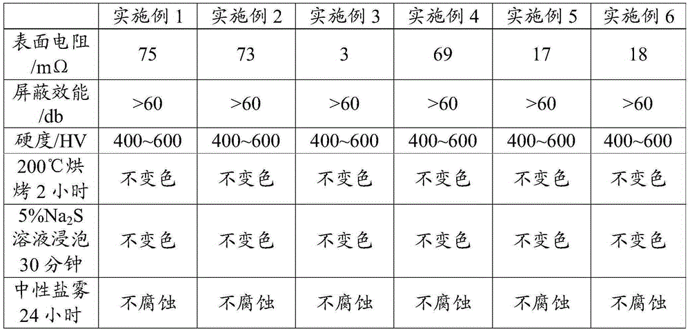
Embodiment 1

[0060] An electromagnetic wave shielding film, comprising a carrier film, an insulating layer, a shielding improvement layer, a shielding effect layer, a shielding protection layer and an adhesive layer compounded sequentially from bottom to top; the thickness of the carrier film is 42 microns; the insulating layer The thickness is 6 microns; the thickness of the shielding improvement layer is 0.005 microns; the thickness of the shielding effectiveness layer is 0.08 microns; the thickness of the shielding protective layer is 0.075 microns; the thickness of the adhesive layer is 7 microns.

Embodiment 2

[0062] An electromagnetic wave shielding film, comprising a carrier film, an insulating layer, a shielding improvement layer, a shielding effectiveness layer, a shielding protection layer and an adhesive layer compounded sequentially from bottom to top; the thickness of the carrier film is 25 microns; the insulating layer The thickness is 2 microns; the thickness of the shielding improvement layer is 0.001 microns; the thickness of the shielding effectiveness layer is 0.08 microns; the thickness of the shielding protection layer is 0.075 microns; the thickness of the adhesive layer is 3 microns.


PUM

PropertyMeasurementUnit
thicknessaaaaaaaaaa
thicknessaaaaaaaaaa
thicknessaaaaaaaaaa

Abstract

The invention relates to an electromagnetic wave shielding film, and the film includes a shielding improvement layer, a shielding efficiency layer and a shielding protection layer which are sequentially compounded from bottom to top. The invention further provides a printed circuit board including the electromagnetic wave shielding film, and a preparation method of the circuit board. The electromagnetic wave shielding film provided by the invention has the advantages of good shielding efficiency, high abrasion resistance, ageing resistance and anti-deformation capacity and the like. The printed circuit board has good shielding property; the preparation method is easy to operate; and industrial production application is facilitated.

Description

technical field [0001] The invention relates to the field of electronic components, in particular to an electromagnetic wave shielding film, a printed circuit board containing the shielding film and a preparation method of the circuit board. Background technique [0002] With the rapid development of the electronics industry, electronic products are further developed toward miniaturization, light weight, and high-density assembly, which greatly promotes the development of flexible circuit boards, thereby realizing the integration of component devices and wire connections. Flexible circuit boards can be widely used in mobile phones, liquid crystal displays, communications, aerospace and other industries. [0003] Driven by the international market, functional flexible circuit boards dominate the flexible circuit board market, and an important indicator of functional flexible circuit boards is electromagnetic shielding (EMIShielding). With the integration of functions of comm...

Claims


Application Information

Patent Timeline
Patent Type & Authority Applications(China)
IPC IPC(8): H05K9/00B32B15/04H05K1/02H05K3/00
Inventor 朱春芳张业朱美芳
Owner 朱春芳
Why Eureka
Try Eureka