A detector for an emission imaging device
A technology of imaging equipment and detectors, applied in the field of detectors, to achieve accurate and orderly installation, and to achieve the effect of overall hermetic packaging
- Summary
- Abstract
- Description
- Claims
- Application Information
AI Technical Summary
Problems solved by technology
Method used
Image
Examples
Embodiment 1
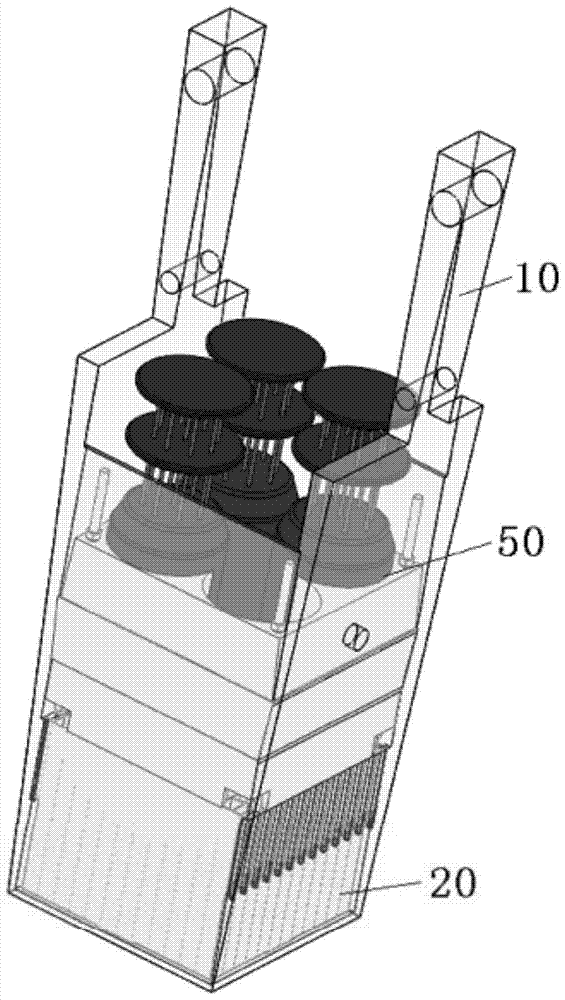
[0057] Such as figure 1 As shown, Embodiment 1 of the present invention includes a packaging box 10, a grid mold 20 and a light sensor assembly 50;
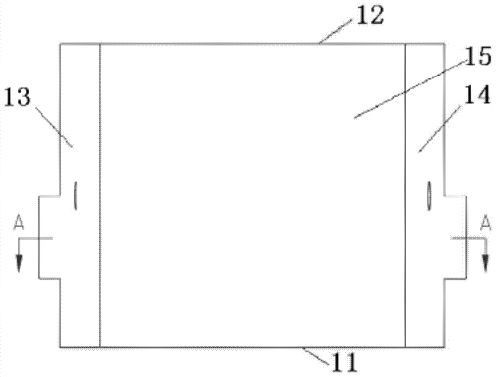
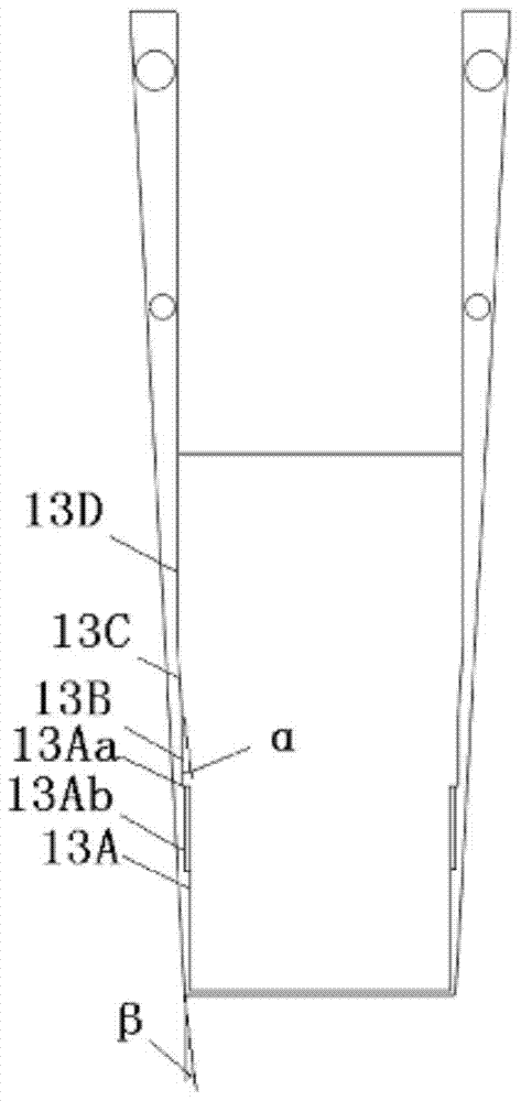
[0058] As shown in Figure 2 (a), Figure 2 (b), and Figure 2 (c), the packaging box 10 is a hollow box body, including a front side 11, a rear side 12, a left side 13, a right side 14 and Bottom surface 15, described front side 11, rear side 12 are vertically connected with bottom surface 15 respectively, the bottom edge of left side 13 and right side 14 is connected with bottom surface 15, front side 11, rear side 12, left side 13, right side The sides of the side surface 14 are sequentially connected to form a closed ring;
[0059] As shown in Figure 2(b) and Figure 2(c), the inner surface of the left side 13 is composed of a lower plane 13A, a middle plane 13B, an inclined plane 13C and an upper plane 13D sequentially spliced from bottom to top. The plane 13A, the middle plane 13B and the upper plane 13D are parallel to eac...
Embodiment 2
[0080] Embodiment 2 of the present invention, its structure, composition are basically the same as Embodiment 1, the difference only lies in:
[0081] The left side 13 of the packaging box 10 has an angle α=30° between the slope 13B and the lower plane 13A;
[0082] The grid mold 20 is a vertical and horizontal grid composed of 19 vertical partitions 21 and 19 horizontal partitions 22 connected vertically, and the 19 longitudinal partitions 21 and 19 horizontal partitions 22 form 20 in the packaging box 10 ×20 grids, each grid is embedded with strip scintillation crystals 30, forming a 20×20 crystal array;
[0083] In this embodiment, the photosensor 51 is a silicon photomultiplier tube (SiPM) with a cylindrical shape, 3×3 in total, and the 3×3 photosensors are arranged close to each other to form a 3×3 photosensor array;
[0084] The shape of the mounting hole 52A of the positioning member 52 is adapted to the outer contour of the side surface of the 3×3 photosensor array; ...
PUM
 Abstract
Description
Claims
Application Information


