Double-sided emission quantum dot light emitting diode and manufacturing method thereof

A quantum dot light-emitting and double-sided light-emitting technology, which is applied in semiconductor/solid-state device manufacturing, electrical components, circuits, etc., can solve the problems of complex manufacturing process, double-sided light-emitting device quality and thickness increase, and achieve quality and thickness reduction. small effect

Active Publication Date: 2016-02-03
TCL CORPORATION
View PDF3 Cites 10 Cited by
  • Summary
  • Abstract
  • Description
  • Claims
  • Application Information

AI Technical Summary

Problems solved by technology

[0006] In view of the above-mentioned deficiencies in the prior art, the purpose of the present invention is to provide a double-sided light-emitting quantum dot light-emitting diode and its preparation method, aiming to solve the problem that the existing double-sided light-emitting device preparation process is relatively complicated, and the existing double-sided light-emitting device The problem of mass and thickness increase

Method used


Image

  • Double-sided emission quantum dot light emitting diode and manufacturing method thereof
  • Double-sided emission quantum dot light emitting diode and manufacturing method thereof
  • Double-sided emission quantum dot light emitting diode and manufacturing method thereof

Examples


Embodiment Construction

[0027] The present invention provides a double-sided light-emitting quantum dot light-emitting diode and its preparation method. In order to make the purpose, technical solution and effect of the present invention clearer and clearer, the present invention will be further described in detail below. It should be understood that the specific embodiments described here are only used to explain the present invention, not to limit the present invention.

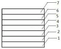
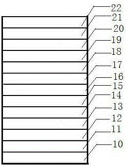
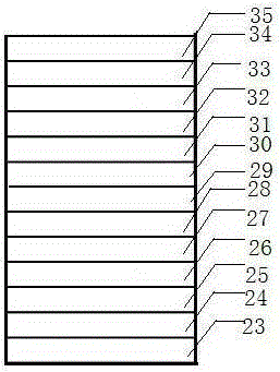
[0028] The double-sided light-emitting quantum dot light-emitting diode of the present invention includes two types of structures: the double-sided light-emitting quantum dot light-emitting diode of the front-mounted structure and the double-sided light-emitting quantum dot light-emitting diode of the flip-chip structure.

[0029] A double-sided light-emitting quantum dot light-emitting diode of the present invention, the double-sided light-emitting quantum dot light-emitting diode is a double-sided light-emitting quantum dot light...


PUM


Abstract

The invention discloses a double-sided emission quantum dot light emitting diode and a manufacturing method thereof. The double-sided emission quantum dot light emitting diode comprises a substrate, a first anode layer, a first hole injection layer, a first hole transfer layer, a first quantum dot light emitting layer, a first electron transfer layer, a first cathode layer, a second anode layer, a second hole injection layer, a second hole transfer layer, a second quantum dot light emitting layer, a second electron transfer layer and a second cathode layer, wherein the first anode layer, the first hole injection layer, the first hole transfer layer, the first quantum dot light emitting layer, the first electron transfer layer and the first cathode layer are arranged on the upper surface of the substrate from bottom to top, and the second anode layer, the second hole injection layer, the second hole transfer layer, the second quantum dot light emitting layer, the second electron transfer layer and the second cathode layer are arranged on the lower surface of the substrate from top to bottom. In addition, the manufacturing method in which a dip-coating method process is used for preparing the quantum dot light emitting diode from the two sides of the substrate at the same time is easier than a manufacturing process of the double-sided emission quantum dot light emitting diode in which quantum dot light emitting diode is prepared from one side of the substrate; and the double-sided emission quantum dot light emitting diode prepared according to the method disclosed by the invention is thinner than a double-sided emission quantum dot light emitting diode prepared according to a mounting process.

Description

technical field [0001] The invention relates to the technical field of quantum dot light emitting diodes, in particular to a double-sided light emitting quantum dot light emitting diode and a preparation method thereof. Background technique [0002] Quantum dots (QD), also known as semiconductor nanocrystals, are a new type of semiconductor nanomaterials. Due to their size smaller than or close to the excitonic Bohr radius, they exhibit strong quantum confinement effects, giving them unique photoluminescent and electroluminescent properties. Compared with other fluorescent materials, quantum dots have excellent optical properties such as high quantum yield, good stability, high color purity, and easy adjustment of luminous color. [0003] Quantum dot light-emitting diode (QLED) is an electroluminescent device that uses quantum dot materials as the light-emitting layer. It inherits the excellent optical properties of quantum dot materials and has important commercial applica...

Claims


Application Information

Patent Timeline
IPC IPC(8): H01L51/50H01L51/56
CPCH10K50/115H10K2102/3031H10K71/00
Inventor 陈亚文
Owner TCL CORPORATION
Why Eureka
Try Eureka