Array substrate and liquid crystal display panel

A technology of liquid crystal display panels and array substrates, applied in nonlinear optics, instruments, optics, etc., can solve the problems of lower product yield, difficult manufacturing process, defects, etc., and achieve the effect of reducing the depth and reducing the occurrence of defects

Active Publication Date: 2016-02-10
TCL CHINA STAR OPTOELECTRONICS TECH CO LTD
View PDF4 Cites 5 Cited by
  • Summary
  • Abstract
  • Description
  • Claims
  • Application Information

AI Technical Summary

Problems solved by technology

[0002] In the current thin-film transistor liquid crystal display panel industry, the technology of manufacturing a color filter film (ColorFilterOnArray, COA) on an array substrate can increase the aperture ratio of the liquid crystal display panel and improve the display quality of the thin film transistor. On the array substrate and in the middle of the protective layer, the contact hole 200 needs to cr

Method used


Image

  • Array substrate and liquid crystal display panel
  • Array substrate and liquid crystal display panel
  • Array substrate and liquid crystal display panel

Examples


Embodiment Construction

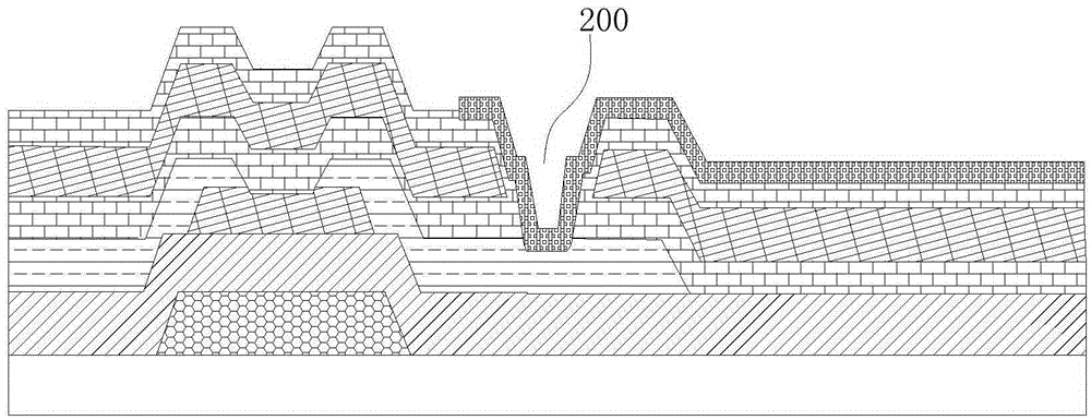
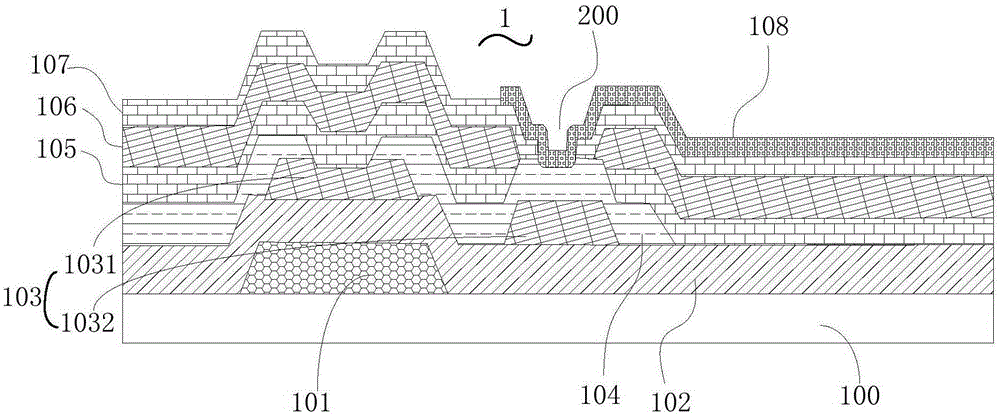
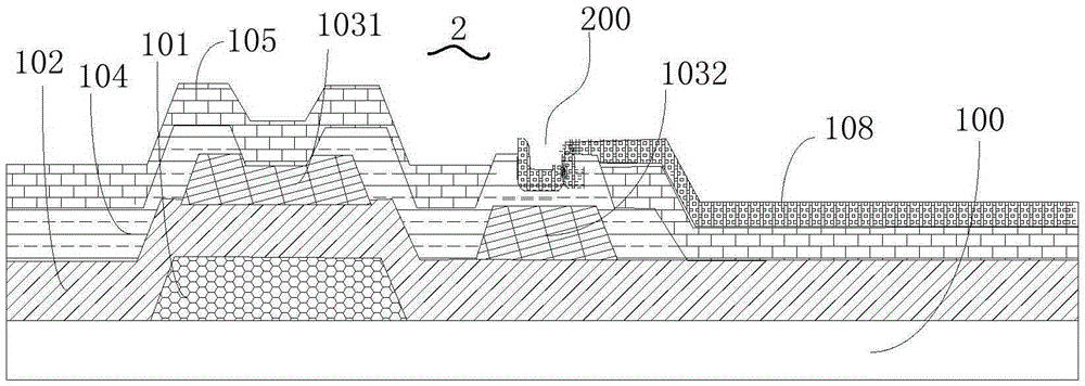
[0035] see figure 2 , is a schematic cross-sectional structure diagram of the array substrate 1 of the present invention. The array substrate 1 includes: a substrate 100; a first metal layer 101, the first metal layer 101 is disposed on the surface of the substrate 100; a first insulating layer 102, the first insulating layer 102 is disposed on On the first metal layer 101, used to isolate the first metal layer 101 and a second metal layer 104; the second metal layer 104 is disposed on the first insulating layer 102; a semiconductor layer 103, The semiconductor layer 103 is disposed between the first insulating layer 102 and the second metal layer 104, the semiconductor layer 103 includes a first semiconductor region 1031 and a second semiconductor region 1032 arranged at intervals, wherein the first A semiconductor region 1031 is used for conducting electricity, and the second semiconductor region 1032 is used to raise the second metal layer; a second insulating layer 105, ...


PUM


Abstract

The invention discloses an array substrate and a liquid crystal display panel. The array substrate comprises a substrate, a first metal layer, a first insulating layer, a second metal layer, a semiconductor layer, a second insulating layer and a pixel electrode layer; the first metal layer comprises grid electrodes of thin film transistors and scanning lines and is arranged on the surface of the substrate; the first insulating layer is arranged on the first metal layer; the second metal layer comprises source electrodes and drain electrodes of the thin film transistors and data lines and is arranged above the first insulating layer; the semiconductor layer comprises a first semiconductor region and a second semiconductor region which are arranged in a spaced mode and is arranged between the first insulating layer and the second metal layer, the first semiconductor region is used for electric conduction, and the second semiconductor region is used for blocking up the second metal layer; the second insulating layer is arranged on the second metal layer; the pixel electrode layer comprises pixel electrodes and common electrodes and is arranged on the second insulating layer. Each contact hole is correspondingly formed in the upper portion of the second semiconductor region and penetrates through the second insulating layer, and the pixel electrode layer is connected with the second metal layer through the contact holes, so that the depth of the contact holes is reduced, and faults caused by too large depth of the contact holes are reduced.

Description

technical field [0001] The invention relates to the field of display technology, in particular to an array substrate and a liquid crystal display panel. Background technique [0002] In the current thin-film transistor liquid crystal display panel industry, the technology of manufacturing a color filter film (ColorFilterOnArray, COA) on an array substrate can increase the aperture ratio of the liquid crystal display panel and improve the display quality of the thin film transistor. On the array substrate and in the middle of the protective layer, the contact hole 200 needs to cross the color resistance of the filter film to be connected to the signal line (such as figure 1 As shown), in order to achieve the purpose of display, since the contact hole 200 needs to cross the color resistance, the depth of the contact hole is greatly increased, which increases the difficulty of the manufacturing process, and easily leads to the occurrence of defects, reducing the yield of the pr...

Claims


Application Information

Patent Timeline
IPC IPC(8): G02F1/1362G02F1/1333G02F1/1343
CPCG02F1/133345G02F1/134363G02F1/13439G02F1/1362G02F1/136227G02F1/136222
Inventor 高冬子
Owner TCL CHINA STAR OPTOELECTRONICS TECH CO LTD
Why Eureka
Try Eureka