Preparation method of integrated circuit chip failure analysis sample

A technology for failure analysis samples and integrated circuits, which is applied in the preparation of test samples, circuits, electrical components, etc., and can solve the problems of no packaging equipment, etc.

Active Publication Date: 2016-02-17
CSMC TECH FAB2 CO LTD
View PDF5 Cites 8 Cited by
  • Summary
  • Abstract
  • Description
  • Claims
  • Application Information

AI Technical Summary

Problems solved by technology

[0003] However, generally only the packaging factory has the ability to package the chip, WaferFoundry's failure analysis laboratory does not have special packaging equipment

Method used


Image

  • Preparation method of integrated circuit chip failure analysis sample
  • Preparation method of integrated circuit chip failure analysis sample
  • Preparation method of integrated circuit chip failure analysis sample

Examples


Embodiment Construction

[0020] In order to make the objects, features and advantages of the present invention more comprehensible, specific implementations of the present invention will be described in detail below in conjunction with the accompanying drawings.

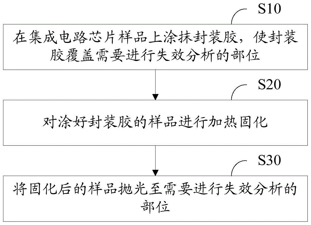
[0021] figure 1 It is a flowchart of a method for preparing samples for failure analysis of integrated circuit chips in an embodiment.

[0022] S10, apply encapsulation glue on the integrated circuit chip sample, so that the encapsulation glue covers the parts to be subjected to failure analysis.

[0023] For the case where the sample is large and does not require positioning analysis, the operator can polish to the desired position more accurately without relying on the mark during subsequent polishing, so an appropriate amount of encapsulant can be directly applied to the sample. Common gluing tools such as brushes and needles can be used for gluing.

[0024] S20, heating and curing the sample coated with encapsulant.

[0025] Heat with...


PUM


Abstract

The invention relates to a preparation method of an integrated circuit chip failure analysis sample. The method includes the following steps: smearing a packaging glue on the integrated circuit chip sample to cover the part required for failure analysis by the packaging glue; heat-curing the sample with packaging glue; and polishing the cured sample until part requiring failure analysis. The method uses cured packaging glue to strengthen the part requiring failure analysis, so as to avoid deformation in the polishing process, and preserve the original appearance. The preparation process does not need expensive equipment and the preparation conditions can be met easily.

Description

technical field [0001] The invention relates to a semiconductor device, in particular to a method for preparing an integrated circuit chip failure analysis sample. Background technique [0002] Due to manufacturing cost considerations, copper wires are used by more and more companies in the wire bonding process of integrated circuit (IC) chips. However, the inherent hardness and easy corrosion of copper wires make the copper wire bonding process have higher requirements on the aluminum thickness of the chip, and failure phenomena such as peeling, craters, and cracks are also prone to occur during the bonding process. Therefore, the demand for failure analysis for copper wire bonding failure is also increasing. Sectional morphology analysis is a commonly used analysis method, and a traditional solution is to polish and observe the morphology after packaging the die. [0003] However, generally only packaging factories have the ability to package chips, and WaferFoundry's fa...

Claims


Application Information

Patent Timeline
Patent Type & Authority Applications(China)
IPC IPC(8): G01N1/28G01N1/32H01L21/02
Inventor 金志明
Owner CSMC TECH FAB2 CO LTD
Why Eureka
Try Eureka