
Semiconductor structures and methods of forming them

A technology of semiconductor and gate structure, applied in the field of semiconductor structure and its formation, can solve the problems of reduced operating speed of semiconductor devices, large influence of MOS transistor performance, large contact resistance, etc., and achieve the effect of reducing the Schottky barrier

Active Publication Date: 2018-08-10
SMIC INT NEW TECH DEV SHANGHAI CO LTD
View PDF4 Cites 0 Cited by
  • Summary
  • Abstract
  • Description
  • Claims
  • Application Information

AI Technical Summary

Problems solved by technology

In the contact resistance of the MOS transistor, due to the small area of ​​the source and the drain, the contact resistance between the metal plug and the metal plug is relatively large, which has a great impact on the performance of the MOS transistor and greatly reduces the operating speed of the semiconductor device.

Method used


Image

  • Semiconductor structures and methods of forming them
  • Semiconductor structures and methods of forming them
  • Semiconductor structures and methods of forming them

Examples


Embodiment Construction

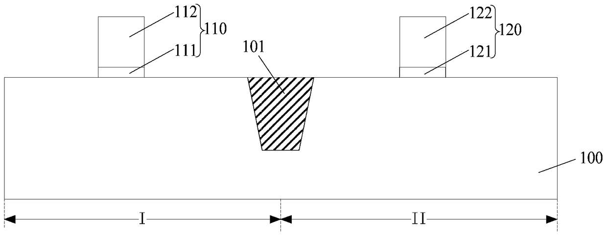
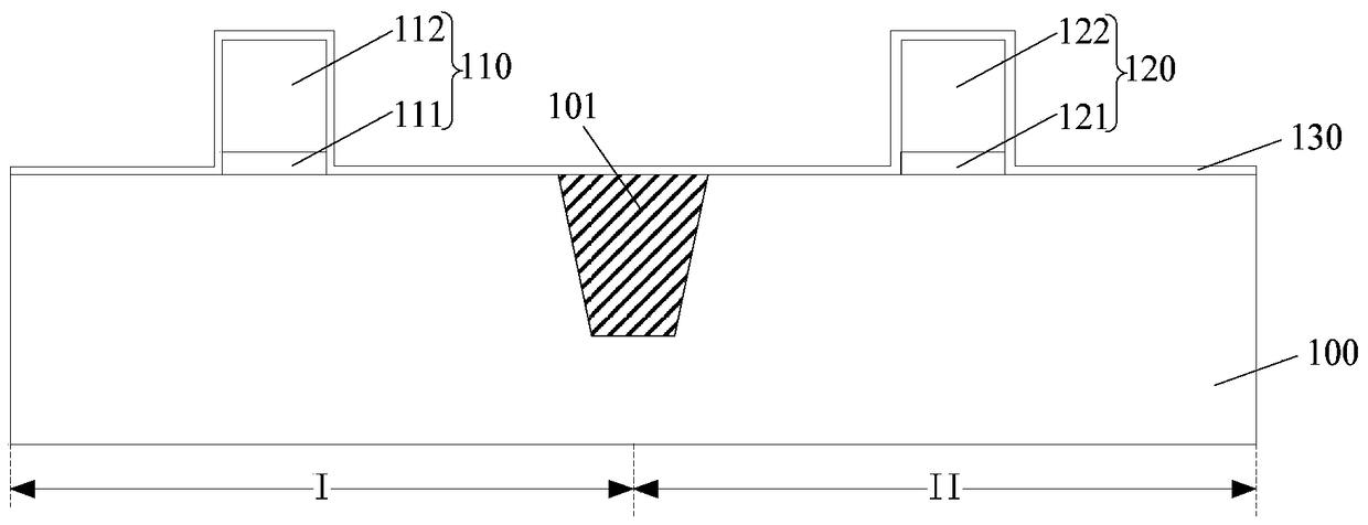
[0030] As mentioned in the background art, the contact resistance of the transistor formed in the prior art needs to be further reduced. Since the contact resistance between the source and drain of the transistor and the metal plug accounts for the main part of the contact resistance of the transistor, it can be further reduced by The contact resistance between the source drain and the metal plug is used to reduce the contact resistance of the transistor.

[0031] Studies have found that when the metal silicide layer is directly formed on the surface of the source and drain, due to the low resistance of the metal silicide layer and the small work function difference with the source and drain, the metal silicide layer and the source and drain There is a lower Schottky barrier between them, so that the contact resistance between the metal silicide layer and the source and drain can be reduced. However, in actual devices, the surface of the source and drain has many defects, such...


PUM


Abstract

The invention discloses a semiconductor structure and a forming method thereof. The forming method of the semiconductor structure comprises the steps as follows: a semiconductor substrate is provided; a gate structure which covers partial surface of the semiconductor substrate is formed; a source and a drain are respectively formed in the semiconductor substrate at two sides of the gate structure; a dielectric layer is formed on the semiconductor substrate; the surface of the dielectric layer is higher than the top surface of the gate structure; a through hole is formed in the dielectric layer and exposes the surfaces of the source and the drain; an oxidation layer is formed on the surfaces of the source and the drain at the bottom of the through hole; a metal material layer is formed on the surface of the oxidation layer; an annealing treatment is carried out; the metal material layer reacts with the oxidation layer to form a metal oxide layer and a metal semiconductor compound layer; and the metal semiconductor compound layer is located on the surface of the metal oxide layer. The contact resistance between the source and the drain of the semiconductor structure formed by the method and the metal semiconductor compound layer is relatively small.

Description

technical field [0001] The invention relates to the technical field of semiconductors, in particular to a semiconductor structure and a forming method thereof. Background technique [0002] With the continuous development of semiconductor technology, the size of semiconductor devices continues to shrink. As the size of the semiconductor device shrinks, the contact resistance of the MOS transistor has an increasing impact on the performance of the MOS transistor and the entire semiconductor chip. In order to improve the performance of semiconductor chips, it is necessary to reduce the contact resistance of MOS transistors. In the contact resistance of the MOS transistor, due to the small area of ​​the source and the drain, the contact resistance between the metal plug and the metal plug is relatively large, which greatly affects the performance of the MOS transistor and greatly reduces the operating speed of the semiconductor device. [0003] Formation process of salicide T...

Claims


Application Information

Patent Timeline
Patent Type & Authority Patents(China)
IPC IPC(8): H01L21/336H01L21/28H01L29/78H01L29/45
Inventor 谢欣云
Owner SMIC INT NEW TECH DEV SHANGHAI CO LTD
Learn More