Semiconductor structure and formation method therefor

A technology of semiconductor and interconnect structure, applied in the direction of semiconductor device, semiconductor/solid-state device manufacturing, semiconductor/solid-state device components, etc., can solve the problems of unstable electrical performance and poor reliability of through-silicon vias

Inactive Publication Date: 2016-02-17
SEMICON MFG INT (SHANGHAI) CORP
View PDF3 Cites 7 Cited by
  • Summary
  • Abstract
  • Description
  • Claims
  • Application Information

AI Technical Summary

Problems solved by technology

[0010] However, the through-silicon vias formed by the existing t

Method used


Image

  • Semiconductor structure and formation method therefor
  • Semiconductor structure and formation method therefor
  • Semiconductor structure and formation method therefor

Examples


Embodiment Construction

[0039] As described in the background art, the through silicon vias formed in the prior art have poor reliability and unstable electrical properties.

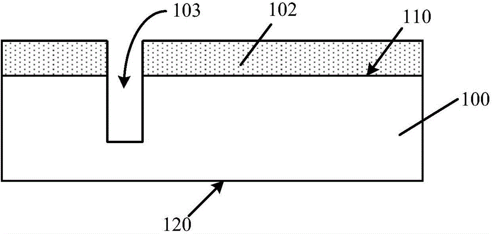
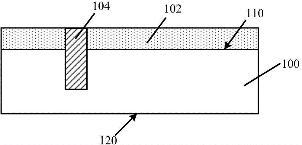
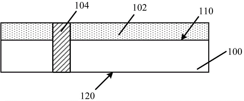
[0040] After research, please continue to refer to Figure 1 to Figure 3 The material of the conductive plug 104 formed in the through hole 103 is metal, such as copper, and the semiconductor substrate 100 is usually a silicon substrate. Due to the difference in thermal expansion coefficient between the metal material and the silicon material, when the conductive When the plug 104 is heated or cooled in the process, there will be a difference in the volume change between the conductive plug 104 and the semiconductor substrate 100, resulting in a gap between the conductive plug 104 and the semiconductor substrate 100 in contact. stress. Moreover, since the conductive plug 104 is used to form a through silicon via structure, the conductive plug 104 needs to penetrate the semiconductor substrate 100 after the second surface 120 of the...


PUM


Abstract

The invention discloses a semiconductor structure and a formation method therefor. The formation method comprises the steps that a substrate is provided, wherein the substrate is provided with a first surface and a second surface that are opposite; a first plug is formed in the substrate, wherein the first plug is provided with a first end and a second end; the first end of the first plug is flush with the first surface of the substrate; the second end of the first plug is positioned in the substrate; the length of the first plug is a first size; the second surface of the substrate is thinned after the first plug is formed until the thickness of the substrate is a second size, wherein the second size is larger than the first size; a second plug is formed in the substrate after the second surface of the substrate is thinned, wherein the second plug is positioned in the surface of the second end of the first plug; the top of the second plug is flush with the second surface of the substrate; a conductive plug is formed by the first plug and the second plug; and the conductive plug penetrates through the substrate. The reliability and the stability of the semiconductor structure are improved.

Description

Technical field [0001] The present invention relates to the technical field of semiconductor manufacturing, in particular to a semiconductor structure and a method of forming the same. Background technique [0002] With the continuous development of semiconductor manufacturing technology, the feature size of semiconductor devices continues to decrease, and the integration of chips is getting higher and higher. However, the current two-dimensional packaging structure has been difficult to meet the increasing demand for chip integration, so three-dimensional packaging technology has become a key technology to overcome the bottleneck of chip integration. [0003] The three-dimensional stacking technology based on through silicon vias (TSV) is one of the existing three-dimensional packaging technologies, and the three-dimensional stacking technology based on through silicon vias is one of the main methods to improve the integration of chips. [0004] The three-dimensional stacking techn...

Claims


Application Information

Patent Timeline
IPC IPC(8): H01L21/768H01L23/48
Inventor 沈哲敏李广宁
Owner SEMICON MFG INT (SHANGHAI) CORP
Why Eureka
Try Eureka