Interconnect structure and method of forming the same

A technology of interconnection structure and plasma, which is applied in the manufacture of electrical components, electrical solid devices, semiconductor/solid devices, etc., can solve problems such as poor smoothness, affecting the shape of through holes, and affecting the performance of conductive plugs, etc., to achieve improved Effects of smoothness, improved bond strength, and reduced dents

Active Publication Date: 2018-03-30
SEMICON MFG INT (SHANGHAI) CORP
View PDF3 Cites 0 Cited by
  • Summary
  • Abstract
  • Description
  • Claims
  • Application Information

AI Technical Summary

Problems solved by technology

[0007] However, in the actual operation process, the performance of the interconnection structure still needs to be further improved, combined with reference image 3 As shown in the electron microscope image, in the prior art interconnection structure, when the through holes formed after etching the insulating layer 11, the adhesion layer 15 and the dielectric layer 12, the smoothness of the sidewall 17 of the through holes is poor, Affects the shape of the via hole, thereby affecting the performance of the conductive plug formed in the via hole 17

Method used


Image

  • Interconnect structure and method of forming the same
  • Interconnect structure and method of forming the same
  • Interconnect structure and method of forming the same

Examples


Embodiment Construction

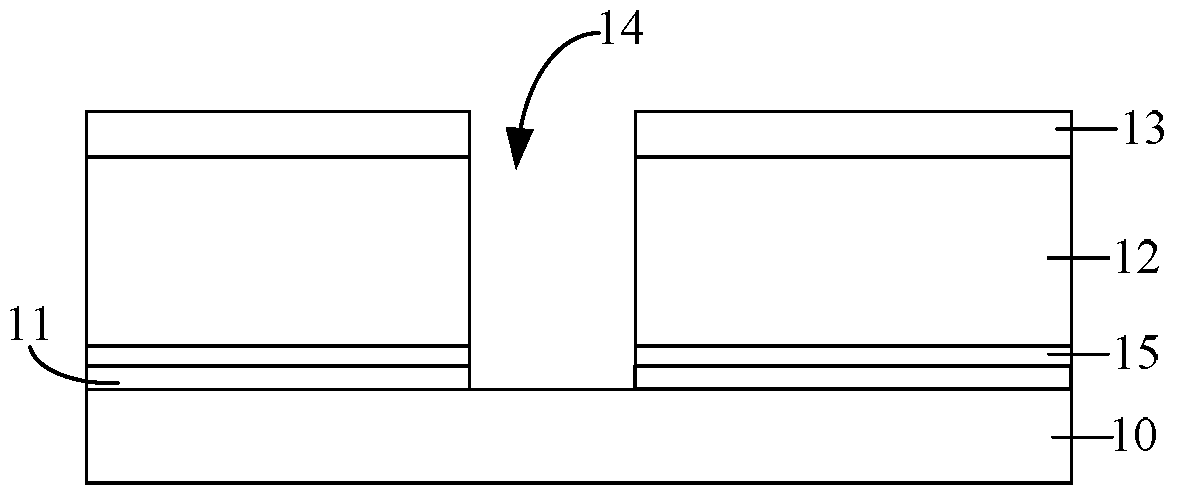
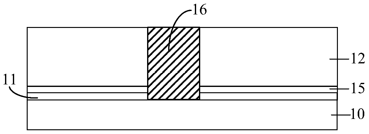
[0054] As mentioned in the background, in the interconnection structure of the prior art, the smoothness of the sidewall of the through hole is poor, which affects the shape of the through hole, and further affects the performance of the interconnection structure.

[0055] Analyzing the reason, in the wet cleaning process after etching the insulating layer, adhesion layer and dielectric layer to form the through hole, the consumption rate of the existing adhesion layer is lower than the consumption rate of the dielectric layer, so the formation of In addition, compared with the technical scheme of directly forming a dielectric layer on the substrate, forming an adhesion layer between the substrate and the dielectric layer can improve the bonding strength of the substrate and the dielectric layer, but in the wet cleaning step, The cleaning solution will still penetrate into the bonding interface of the substrate, the plasma-enhanced silicon oxide adhesion layer and the dielectri...


PUM


Abstract

The invention provides an interconnection structure and a forming method thereof. The method for forming the interconnection structure includes: first using silicon source gas and oxygen source gas to perform plasma treatment on the substrate, forming a plasma-enhanced silicon oxide adhesion layer on the substrate, and then placing the plasma-enhanced silicon oxide on the substrate. A dielectric layer is formed on the adhesion layer, and after the dielectric layer is etched to form a through hole in the dielectric layer and the plasma-enhanced silicon oxide adhesion layer, a conductive plug is formed in the through hole. Compared with the adhesion layer in the prior art, the plasma-enhanced silicon oxide adhesion layer has a larger removal rate in the subsequent process of semiconductor device preparation after the formation of the through hole (such as the wet cleaning process for the through hole) , so that the etching rate of the dielectric layer is equivalent to that of the plasma-enhanced silicon oxide adhesion layer, thereby improving the overall smoothness of the sidewall of the through hole, so as to improve the shape of the sidewall of the through hole.

Description

technical field [0001] The invention relates to the technical field of semiconductors, in particular to an interconnection structure and a forming method thereof. Background technique [0002] With the development of semiconductor technology, the integration level of semiconductor devices continues to increase, and the feature size (Critical Dimension, CD) of semiconductor devices becomes smaller and smaller. [0003] With the gradual reduction of the feature size of semiconductor devices, RC delay (RC delay) caused by parasitic capacitance between interconnection structures has a greater impact on semiconductor devices. Reducing the K value of the dielectric layer material in the interconnection structure is an effective method to reduce the RC delay effect. In recent years, low K dielectric constant (Low K, LK) materials (K<3) and ultra-low K dielectric constant (Ultra Low K, ULK) material to reduce the RC delay problem. [0004] Existing processes for forming interc...

Claims


Application Information

Patent Timeline
Patent Type & Authority Patents(China)
IPC IPC(8): H01L21/768H01L23/532
Inventor 周鸣
Owner SEMICON MFG INT (SHANGHAI) CORP
Why Eureka
Try Eureka