Container array, formation method thereof and semiconductor device

A technology of capacitors and arrays, which is applied to semiconductor devices, electric solid devices, electrical components, etc., can solve the problem of inability to fully form the capacitor dielectric layer and upper electrode, and achieve the effect of increasing the capacitance value

Pending Publication Date: 2018-02-16
CHANGXIN MEMORY TECH INC
View PDF5 Cites 12 Cited by
  • Summary
  • Abstract
  • Description
  • Claims
  • Application Information

AI Technical Summary

Problems solved by technology

[0005] The purpose of the present invention is to provide a capacitor array to solve the problem that the capacitor dielectric layer and the upper electrode cannot be fully formed on the inner surface of the lower electrode in the existing capacitor array

Method used


Image

  • Container array, formation method thereof and semiconductor device
  • Container array, formation method thereof and semiconductor device
  • Container array, formation method thereof and semiconductor device

Examples


Embodiment 1

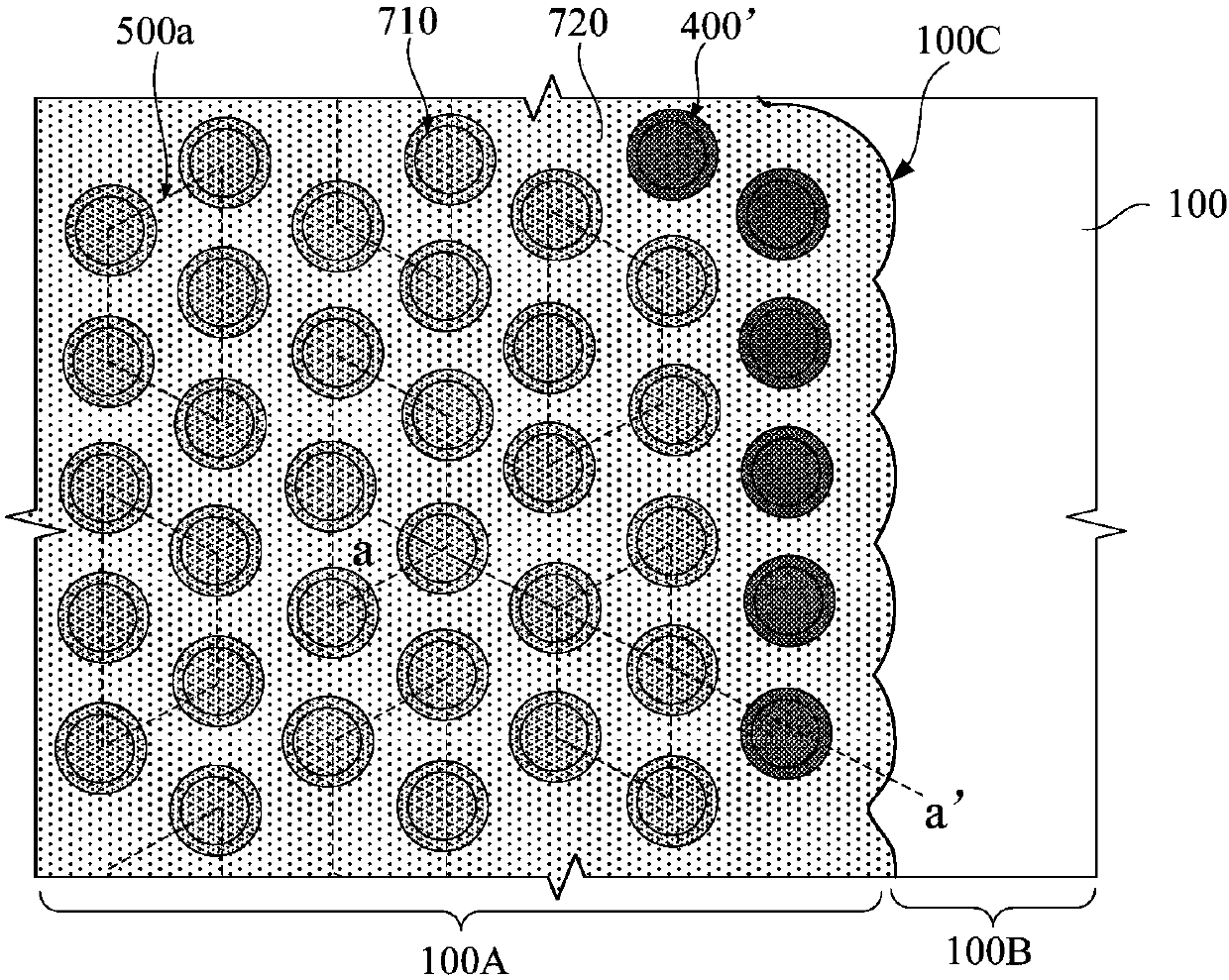
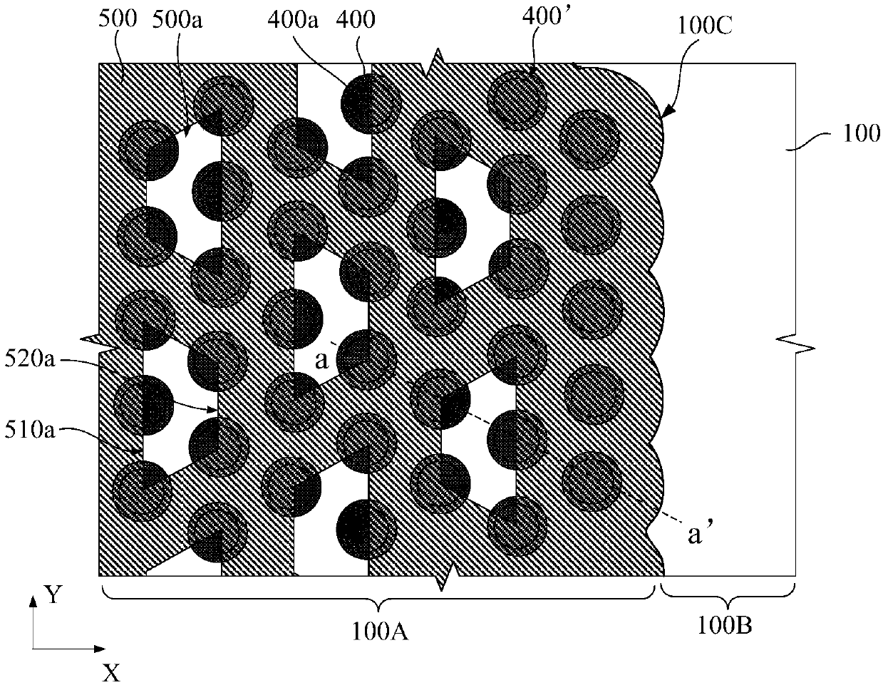
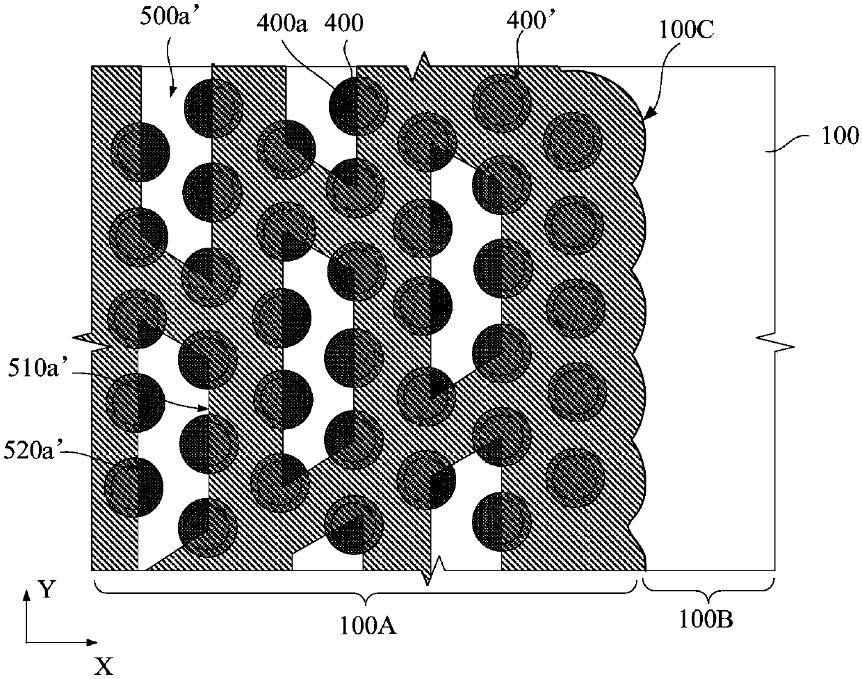
[0096] Figure 1a is a top view of the capacitor array in Embodiment 1 of the present invention, Figure 1b It is a schematic diagram of an electrode group layer in a capacitor array in Embodiment 1 of the present invention, Figure 1c It is a schematic diagram of another electrode group layer in the capacitor array in the first embodiment of the present invention, Figure 1d for Figure 1a The shown cross-sectional view of the capacitor array in the first embodiment of the present invention along the aa' direction.

[0097] combine Figure 1a ~ Figure 1c As shown, the capacitor array includes:

[0098] A substrate 100 having a device region 100A formed with the capacitor array;

[0099] A plurality of lower electrodes 400 are disposed on the device region 100A of the substrate 100, and the shape of the lower electrodes 400 includes a cylindrical structure;

[0100]An electrode group layer 500 is arranged on the top port 400a of the tubular structure of the plurality of lo...

Embodiment 2

[0127] figure 2 It is a schematic flow chart of the method for forming the capacitor array in Embodiment 2 of the present invention, as figure 2 As shown, the forming method of capacitor array provided by the present invention comprises:

[0128] Step S110, providing a substrate on which a device region for forming the capacitor array is defined;

[0129] Step S120, forming a sacrificial layer on the substrate, the sacrificial layer is formed with a plurality of through holes arranged in an array corresponding to the part of the device region;

[0130] Step S130, forming a lower electrode in the through hole of the sacrificial layer, the lower electrode covering the bottom and sidewall of the through hole to form a cylindrical structure;

[0131] Step S140, forming an electrode group layer on the top port of the cylindrical structure of the sacrificial layer and the lower electrode, and opening a plurality of through holes in the electrode group layer, each of the through ...

Embodiment 3

[0198] Based on the above capacitor array, the present invention also provides a semiconductor device. The semiconductor device includes a capacitor array as described above.

[0199] Specifically, the semiconductor device may be, for example, a memory, and the memory generally includes a capacitor and a storage transistor connected to the capacitor, and the capacitor is used to store charges representing stored information. Therefore, the semiconductor device may further include a memory cell array, and the memory cells in the memory cell array are electrically connected to the capacitors in the capacitor array. Specifically, the storage cells in the storage cell array are electrically connected to the node contacts, so that the storage cells and capacitors can be electrically connected by using the node contacts.

[0200] In summary, in the capacitor array provided by the present invention, since the through-hole is opened in the layer of the electrode group, and both the i...


PUM


Abstract

The invention provides a container array, a formation method thereof and a semiconductor device. In the container array, a penetrating hole in an electrode group pattern layer communicates with a cylindrical internal part and a cylindrical external part of a cylindrical structure of a lower electrode, the projection of a linear boundary of the penetrating hole in a height direction penetrates through at least one top port of the lower electrode, thus, the area size, corresponding to the penetrating hole, of the top port of the lower electrode still cannot be effected even displacement deviation exists in the penetrating hole in an extension direction of the linear boundary, and a complete capacitance dielectric layer and an upper electrode can be enabled to be formed on an inner surface and an outer surface of the lower electrode. Moreover, the opening size of the penetrating hole is relatively large, so that the corresponding etching rate and the film formation rate are also favorablyimproved during etching an etching process and a film formation process via the penetrating hole.

Description

technical field [0001] The invention relates to the technical field of semiconductors, in particular to a capacitor array, a forming method thereof, and a semiconductor device. Background technique [0002] With the continuous development of semiconductor technology, the performance requirements of capacitors in semiconductor integrated circuits are also getting higher and higher. Capacitors with high reliability have become an important issue. [0003] Generally, a capacitor includes an upper electrode, a capacitive dielectric layer and a lower electrode, and the capacitive dielectric layer is disposed between the upper electrode and the lower electrode. When preparing a capacitor array composed of multiple capacitors, the commonly used method is, for example, as follows: firstly, a lower electrode with a cylindrical structure is formed on the substrate; then an electrode group layer is partially covered on the top port of the lower electrode, so A through hole is opened ...

Claims


Application Information

Patent Timeline
Patent Type & Authority Applications(China)
IPC IPC(8): H01L27/24
CPCH10B63/22
Inventor 不公告发明人
Owner CHANGXIN MEMORY TECH INC
Why Eureka
Try Eureka