Method for polishing gallium nitride crystals

A gallium nitride wafer, gallium nitride technology, applied in surface polishing machine tools, grinding/polishing equipment, semiconductor/solid-state device manufacturing, etc., can solve problems such as poor polishing of gallium nitride crystals, and improve chemical reactions speed, improve polishing efficiency, and solve the effect of difficult polishing

Inactive Publication Date: 2010-03-17
CHINA ELECTRONICS TECH GRP NO 46 RES INST
View PDF0 Cites 16 Cited by
  • Summary
  • Abstract
  • Description
  • Claims
  • Application Information

AI Technical Summary

Problems solved by technology

[0007] The invention provides a method for effectively improving the surface quality of the wafer and obtaining a bright mirror-surface gallium nitride crystal polishing method to solve the problem of poor gallium nitride crystal polishing in the prior art

Method used


Image

  • Method for polishing gallium nitride crystals
  • Method for polishing gallium nitride crystals
  • Method for polishing gallium nitride crystals

Examples


Embodiment Construction

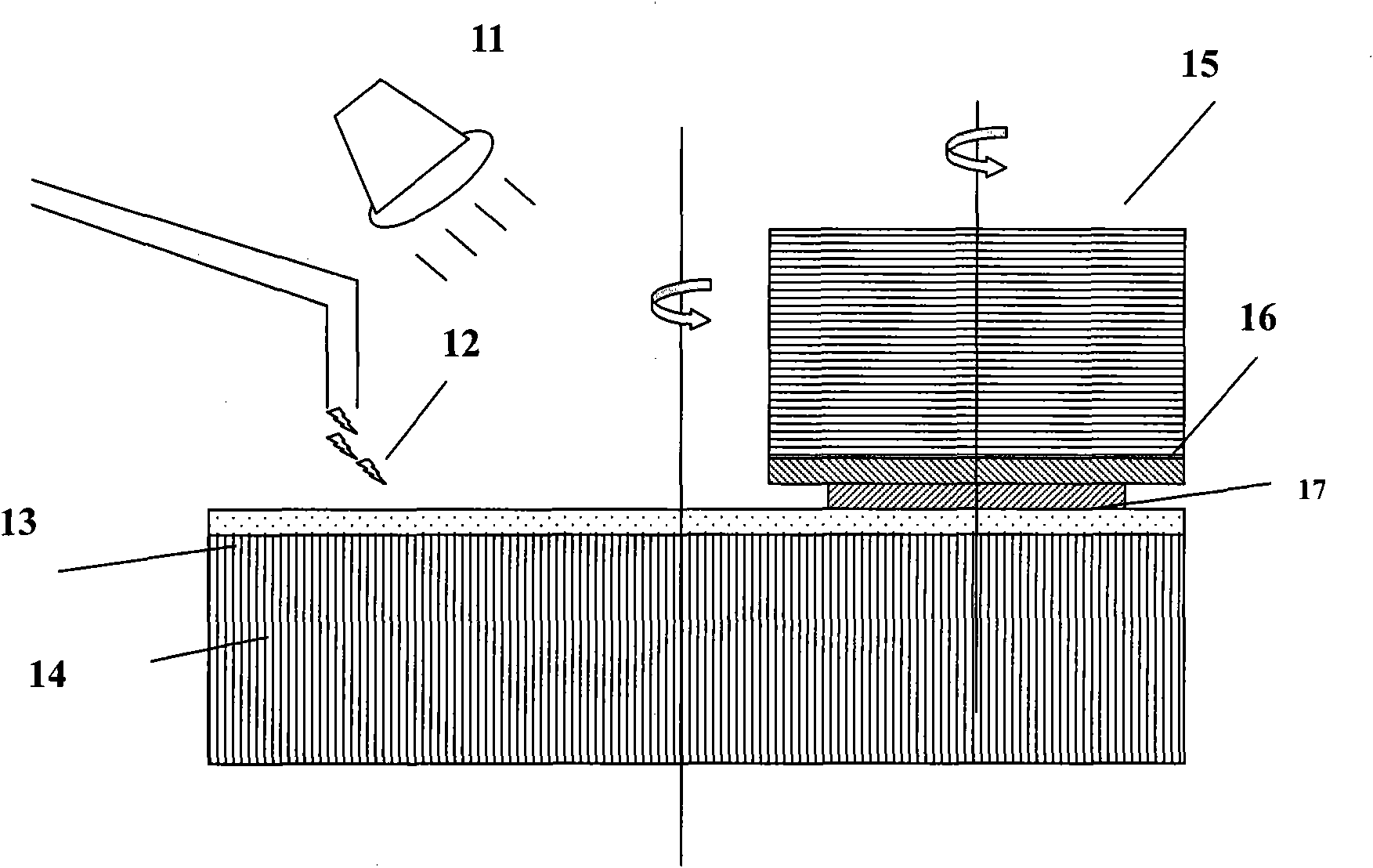
[0029] The present invention will be further described in detail below with reference to the accompanying drawings and embodiments. It should be understood that the specific embodiments described herein are only used to illustrate the present invention, but not to limit the present invention.

[0030] The method for polishing a gallium nitride crystal of this embodiment includes the following steps:

[0031] Step A: Glue the gallium nitride wafer on the quartz plate with high temperature wax.

[0032] Step B: Use a grinder to grind the gallium nitride wafer pasted on the quartz plate.

[0033] Step C: heating the polishing solution by heating in a water bath, irradiating the polished wafer with ultraviolet light, and performing chemical mechanical polishing on the ground gallium nitride wafer with a polishing machine.

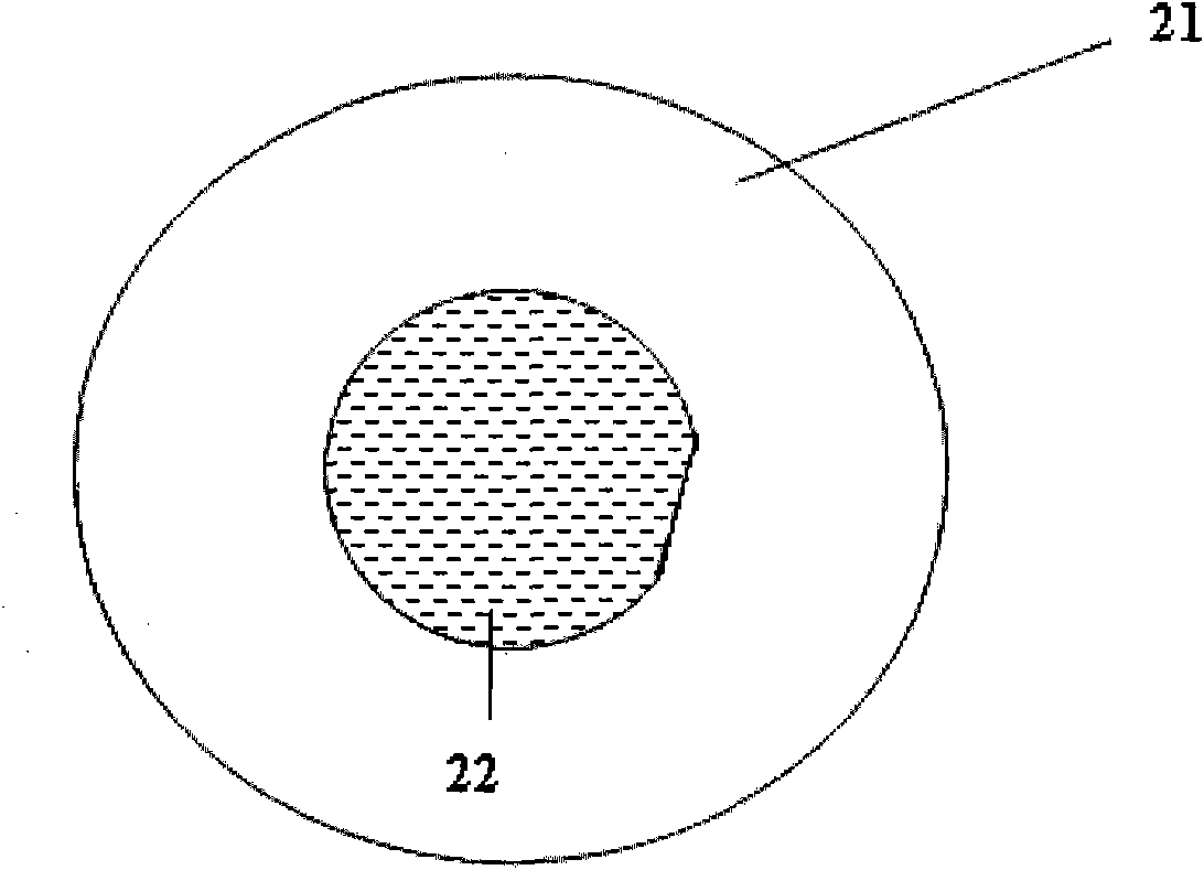
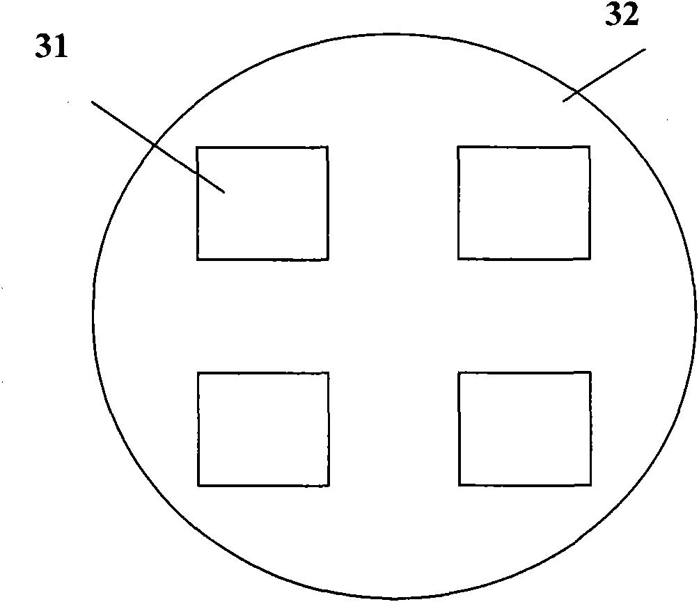
[0034] The sticking method described in step A includes large piece sticking and small piece sticking. like figure 2 As shown, a large GaN wafer 22 (≥2 in...


PUM

PropertyMeasurementUnit
particle diameteraaaaaaaaaa

Abstract

The invention discloses a method for polishing gallium nitride crystals, comprising the following steps: sticking gallium nitride wafers on a quartz plate; grinding the gallium nitride wafers stuck onthe quartz plate by a grinder; heating up the polishing solution, irradiating the polished gallium nitride wafers by ultraviolet light and carrying out chemical mechanical polishing on the ground gallium nitride wafers by a polisher. In the method, based on the chemical mechanical polishing of the traditional gallium nitride wafers, the ultraviolet light is used for irradiating the wafers and a self-made water-bath heating system is simultaneously used for heating up the polishing solution, thus increasing the chemical reaction rate in the process of chemical mechanical polishing, and by adjusting the weight of the heavy objects, the physical removing effect and the chemical effect are balanced, thus not only solving the problem that the gallium nitride wafers are difficult to polish andincreasing the removal rates of N surface and Ga surface, but also obtaining satisfactory shiny surfaces. The method features obviously lower cost and simple process implementation and effectively increases the polishing efficiency.

Description

technical field [0001] The invention relates to the field of semiconductor polishing, in particular to a method for polishing gallium nitride crystals. Background technique [0002] The third-generation semiconductor material gallium nitride has the unique properties of large band gap, high breakdown electric field, high thermal conductivity, high electron saturation drift speed, small dielectric constant, strong radiation resistance, and high chemical stability. Optoelectronic devices such as optical display, optical storage, and optical detection, and microelectronic devices such as high-temperature, high-frequency and high-power electronics have broad application prospects. GaN-based devices have not only been widely used in civilian applications and have huge market potential, but also have great application prospects in the military, and have received great attention from the military of various countries. [0003] In the early and mid-1990s, breakthroughs in GaN-based...

Claims


Application Information

Patent Timeline
Patent Type & Authority Applications(China)
IPC IPC(8): H01L21/00H01L21/302B24B37/04B24B29/02
Inventor 李强徐永宽程红娟殷海丰于祥潞杨丹丹赖占平严如岳
Owner CHINA ELECTRONICS TECH GRP NO 46 RES INST
Why Eureka
Try Eureka