Film transistor substrate and display panel

A thin-film transistor and display panel technology, which is applied in the direction of electric solid-state devices, semiconductor devices, static indicators, etc., can solve the problems of display panel flickering, afterimage, different brightness of thin-film transistor display panels, etc., and achieve the effect of improving hysteresis

Active Publication Date: 2016-02-17
INNOLUX CORP
View PDF4 Cites 6 Cited by
  • Summary
  • Abstract
  • Description
  • Claims
  • Application Information

AI Technical Summary

Problems solved by technology

The hysteresis of the thin film transistor will cause the display panel to produce different brightness under the same grayscale signal, therefore, it will cause the display panel to appear flicker or afterimage

Method used


Image

  • Film transistor substrate and display panel
  • Film transistor substrate and display panel
  • Film transistor substrate and display panel

Examples


Embodiment Construction

[0026] Some exemplary embodiments are shown in the accompanying drawings, and various exemplary embodiments will be described more fully hereinafter with reference to the accompanying drawings. It should be noted that the inventive concept may be embodied in many different forms and should not be construed as limited to the illustrative embodiments set forth herein. Rather, these exemplary embodiments are provided so that this disclosure will be thorough and complete, and will fully convey the scope of the inventive concept to those skilled in the art. In each of the drawings, the relative size ratios may have been exaggerated for clarity of depicted layers and regions, and like numerals indicate like elements throughout.

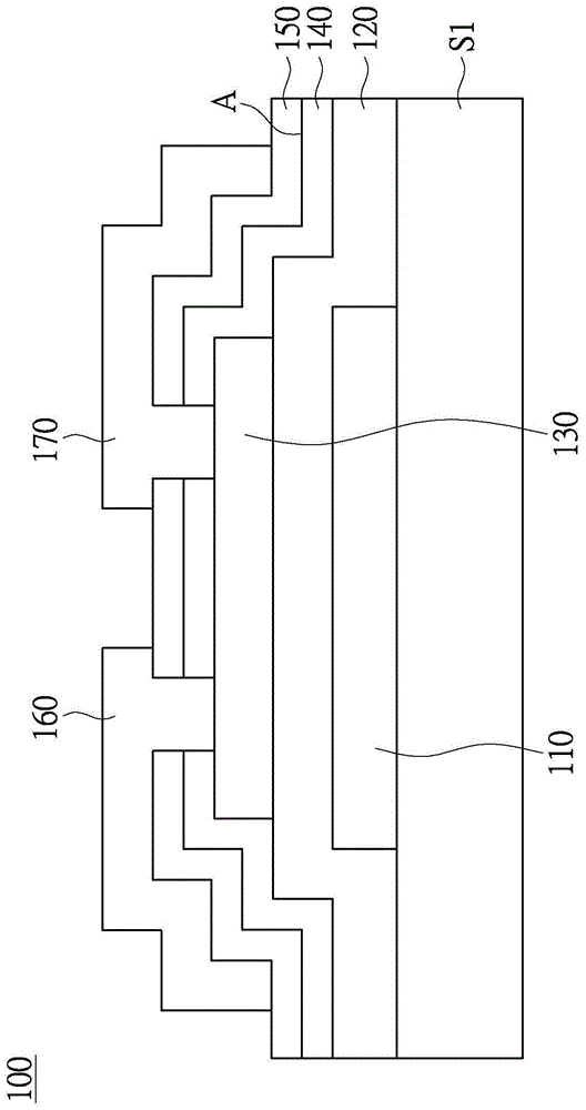
[0027] figure 1 is a schematic cross-sectional view of the thin film transistor according to the first embodiment of the present invention. see figure 1 , in this embodiment, the thin film transistor 100 is a bottom-gate thin film transistor, and include...


PUM


Abstract

The invention relates to a film transistor substrate and a display panel. The substrate provided by the embodiment of the invention comprises a substrate, a grid electrode, a semiconductor layer, a source electrode, a drain electrode, a first protection layer, and a second production layer. The grid electrode is configured to be on the substrate. The semiconductor layer is electrically isolated from the grid electrode. The source electrode and the drain electrode are electrically connected with the semiconductor layer. The first protection layer is configured to be on the semiconductor layer, and is provided with a first oxygen vacancy concentration. The second protection layer is configured to be on the first layer, and is provided with a second oxygen vacancy concentration. A junctional zone is located between the first protection layer and the second protection layer, and has a third oxygen vacancy concentration. The third oxygen vacancy concentration is greater than the first and second oxygen vacancy concentrations.

Description

technical field [0001] The invention relates to a structure of a thin film transistor substrate, and in particular to a thin film transistor substrate applied to a display panel. Background technique [0002] Currently common thin film transistor displays (Thinfilm transistor displays) include active element substrates. The active element substrate is to arrange thin film transistors on the substrate. [0003] When the current change curve when the voltage applied to the thin film transistor changes from low to high and the current change curve when the voltage changes from high to low, it is hysteresis. The hysteresis phenomenon of the thin film transistor will cause the display panel to produce different brightness under the same gray scale signal, thus causing the display panel to flicker or afterimage. Contents of the invention [0004] An embodiment of the present invention provides a thin film transistor, and the first protective layer and the second protective lay...

Claims


Application Information

Patent Timeline
Patent Type & Authority Applications(China)
IPC IPC(8): H01L27/12H01L29/06G09G3/32G09G3/36
CPCH01L27/1248H01L29/0603
Inventor 李冠锋蒋国璋颜子旻
Owner INNOLUX CORP
Why Eureka
Try Eureka