Printed circuit board manufacturing method and printed circuit board

A technology for printed circuit boards and manufacturing methods, which is applied in the fields of printed circuit manufacturing, printed circuits, printed circuits assembled with electric components, etc., and can solve problems such as the unevenness of the back of PCB board 10 and affect the welding effect, so as to achieve good heat dissipation and ensure welding Effect, the effect of ensuring flatness

Inactive Publication Date: 2016-02-17
SHENZHEN VMAX POWER
View PDF5 Cites 10 Cited by
  • Summary
  • Abstract
  • Description
  • Claims
  • Application Information

AI Technical Summary

Problems solved by technology

[0002] like figure 1 As shown, in the conventional PCBA (printed circuit board) production and processing process, in order to improve the current carrying capacity of the SMD power device 20 and enhance the heat dissipation effect, a large area of ​​copper is laid on the top and bottom layers of the PCB board 10 under the SMD power device 20 Skin, in the projection area of ​​the SMD power device 20, a solder resist window is opened to form a pad 30 and an array of heat conduction holes 50. This design has the following disadvantages in the processing process: First, the molten tin 40 passes through the heat conduction holes 50 during reflow soldering. flow to the back of the PCB, resulting in less tin when the SMD power device is soldered, which affects the soldering effect; second, the back of the PCB 10 is uneven after soldering, and there may even be tin tips 60

Method used


Image

  • Printed circuit board manufacturing method and printed circuit board
  • Printed circuit board manufacturing method and printed circuit board
  • Printed circuit board manufacturing method and printed circuit board

Examples


Embodiment Construction

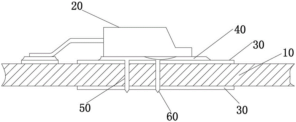
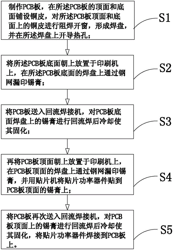
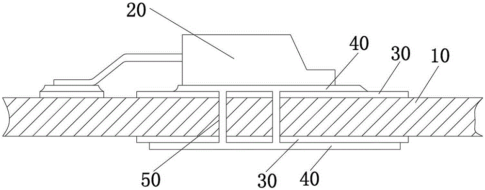
[0020] Such as figure 2 As shown, the method for soldering patch power devices on the PCB proposed by the present invention comprises the following steps: S1, making a PCB, laying copper sheets on the top and bottom surfaces of the PCB, and the copper sheets on the top and bottom surfaces of the PCB Carry out solder resist window opening on the upper surface to form a pad, and open a thermal hole on the pad; S2, place the bottom of the PCB on the printing machine, and print solder paste on the pad on the bottom of the PCB; S3, Send the PCB board into the reflow soldering machine, reflow the solder paste on the pad on the bottom surface of the PCB board, and then cool it to make it solidify; The solder paste is printed on the board, and the chip power device is pasted on the solder paste on the top surface of the PCB board with a mounter; S5, the PCB board is sent to the reflow soldering machine again, and the solder paste on the top surface of the PCB board is reflowed After...


PUM


Abstract

The invention discloses a printed circuit board manufacturing method and a printed circuit board. The method includes the following steps of manufacturing the PCB, lining the top face and the bottom face of the PCB with copper sheets, conducting solder mask opening on the copper sheets of the top face and the bottom face of the PCB to form weld discs, forming heat conduction holes in the weld discs, putting the PCB on a printing machine with the bottom face facing upwards, conducting solder paste skip printing on the weld disc on the bottom face of the PCB through a steel screen, putting the PCB on the printing machine with the top face facing upwards, conducting solder paste skip printing on the weld disc on the top face of the PCB through the steel screen, attaching a chip power device to solder paste of the top face of the PCB through a chip mounter, sending the PCB into a backflow welding machine, cooling and solidifying solder paste on the top face of the PCB after backflow welding, and welding the chip power device to the PCB. The welding effect of the chip power device and the smoothness of the bottom face of the PCB are ensured.

Description

technical field [0001] The invention relates to the field of manufacturing and processing of printed circuit boards, and more specifically relates to a method for manufacturing a printed circuit board and a printed circuit board. Background technique [0002] Such as figure 1 As shown, in the conventional PCBA (printed circuit board) production and processing process, in order to improve the current carrying capacity of the SMD power device 20 and enhance the heat dissipation effect, a large area of ​​copper is laid on the top and bottom layers of the PCB board 10 under the SMD power device 20 Skin, open the solder resist window in the projection area of ​​the patch power device 20 to form the pad 30 and punch the array of heat conduction holes 50. This design has the following disadvantages in the processing process: First, the molten tin 40 passes through the heat conduction holes 50 during reflow soldering. Flow to the back of the PCB, resulting in less tin when the SMD ...

Claims


Application Information

Patent Timeline
Patent Type & Authority Applications(China)
IPC IPC(8): H05K3/34
CPCH05K3/3494H05K2203/043
Inventor 刘钧冯颖盈游丽仙
Owner SHENZHEN VMAX POWER
Why Eureka
Try Eureka