Novel probe-positioning tin soldering device and tin soldering method

A technology of positioning points and probes, applied in welding equipment, welding equipment, laser welding equipment, etc., can solve the problems of slow speed, poor quality of tin spots, and inability to meet laser welding and other problems

Active Publication Date: 2016-03-02
SHENZHEN INTE LASER TECH
View PDF9 Cites 12 Cited by
  • Summary
  • Abstract
  • Description
  • Claims
  • Application Information

AI Technical Summary

Problems solved by technology

[0002] With the wide application of tinning technology for electronic products, the requirements for the amount of tinning are strict, and the spacing between tinning tires is small. The traditional tinning method for electronic products is manual tinning, which is sl

Method used


Image

  • Novel probe-positioning tin soldering device and tin soldering method
  • Novel probe-positioning tin soldering device and tin soldering method
  • Novel probe-positioning tin soldering device and tin soldering method

Examples


Embodiment Construction

[0027] In order to make the object, technical solution and advantages of the present invention clearer, the present invention will be further described in detail below in conjunction with the accompanying drawings and embodiments. It should be understood that the specific embodiments described here are only used to explain the present invention, not to limit the present invention.

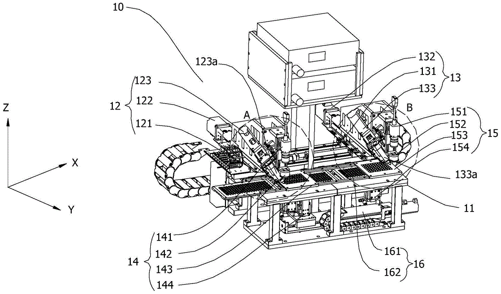
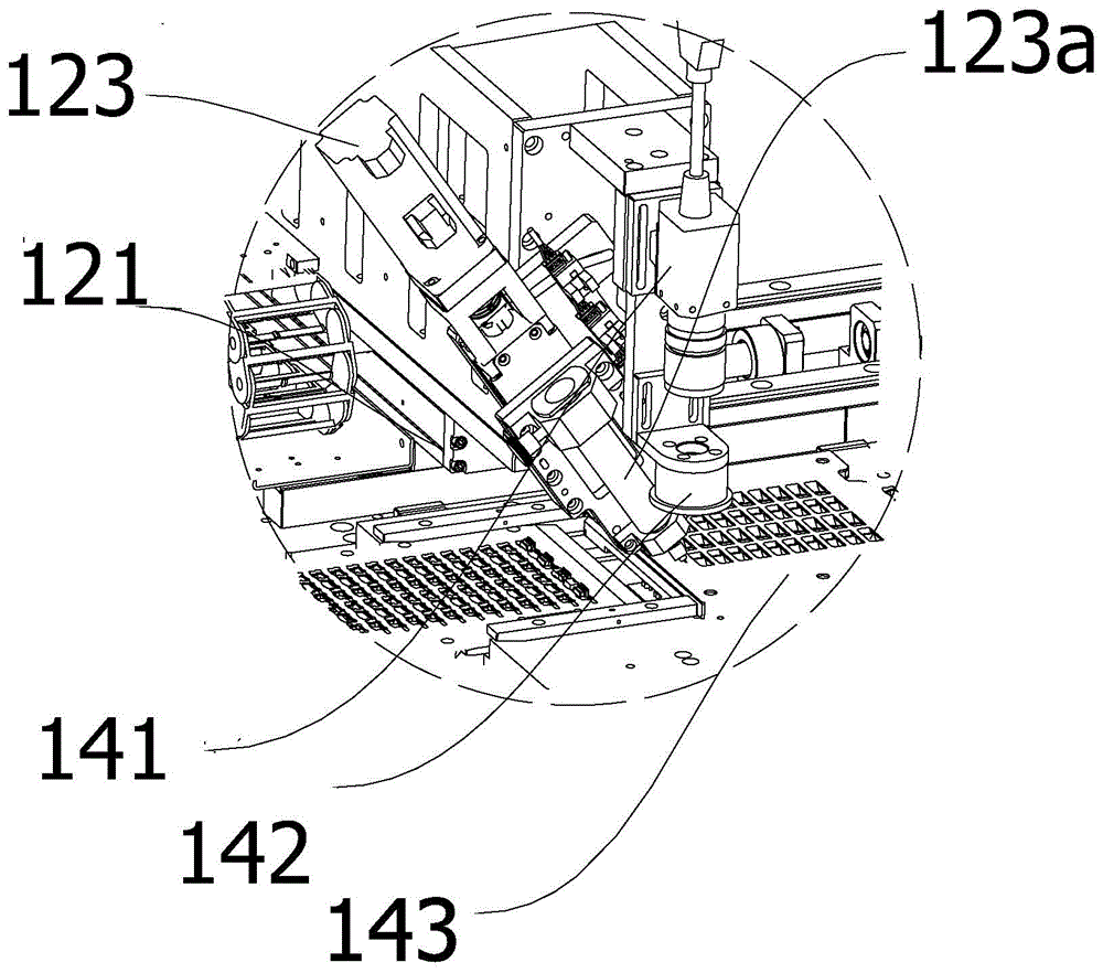
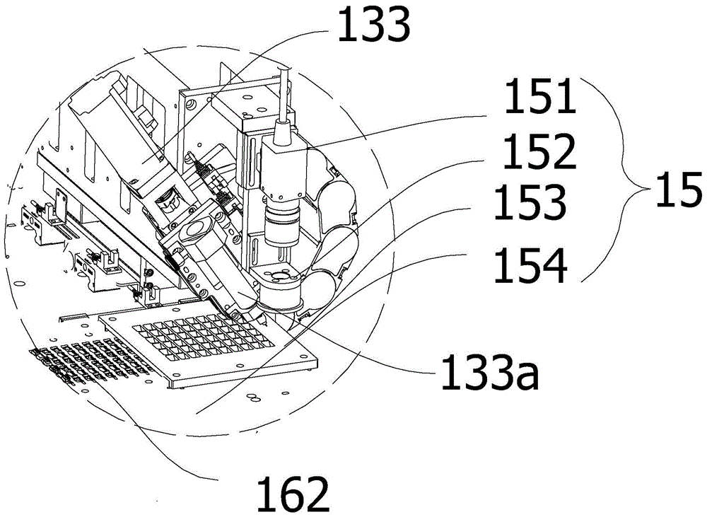
[0028] see figure 1 , figure 2 and image 3 , figure 1 It is a structural representation of the novel probe positioning point tin equipment of the present invention, figure 2 for figure 1 A magnified view of the region A shown, image 3 for figure 1 The enlarged view of the B area shown; in this embodiment, the novel probe positioning point tin device 10 includes a device body 11, a control assembly housed inside the device body 11, and a first point of tin installed on the device body 11. Structural assembly 12, second point tin structural assembly 13, first positioning mechanism 14 assem...


PUM


Abstract

The invention discloses a novel probe-positioning tin soldering device. The novel probe-positioning tin soldering device comprises a device body, a control assembly, a first tin soldering structure assembly, a second tin soldering structure assembly, a first positioning mechanism, a second positioning mechanism and a tray mechanism. The first tin soldering structure assembly and the second tin soldering structure assembly can both move along the X axis, the Y axis and the Z axis relative to the device body. A sliding rail is arranged on the device body. The first tin soldering structure assembly comprises a first tin soldering needle, a second tin soldering needle, a first CCD camera and a plurality of first elastic positioning probes. The second positioning mechanism comprises a second CCD camera, a second tin soldering positioning reference panel and a plurality of second elastic positioning probes. The novel probe-positioning tin soldering device is high in work efficiency, capable of accurately regulating the height of a product to be subjected to tin soldering, high in accuracy, and capable of running in a full automatic manner, accurately positioning tin soldering positions of electronic products and meeting the requirement of laser welding. The invention further discloses a novel probe-positioning tin soldering method.

Description

technical field [0001] The invention relates to the technical field of tin spotting, in particular to novel probe positioning tin spotting equipment and a tin spotting method. Background technique [0002] With the wide application of tinning technology for electronic products, the requirements for the amount of tinning are strict, and the spacing between tinning tires is small. The traditional tinning method for electronic products is manual tinning, which is slow in speed and poor in accuracy, and is far from meeting the requirements of laser welding. Requirements, electronic products are easy to be damaged, tinning is uneven and unsightly, manual processing is required after tinning, poor quality of tin dots, and pores will occur. Contents of the invention [0003] The technical problem to be solved by the present invention is to provide a new type of probe positioning point tin equipment, which has high working efficiency, can accurately adjust the height of the tin pr...

Claims


Application Information

Patent Timeline
IPC IPC(8): B23K3/06B23K3/08B23K26/70
Inventor 邹武兵张德安禹刚曾波余猛
Owner SHENZHEN INTE LASER TECH
Why Eureka
Try Eureka