PCB packaging design and welding method of TQFP chip

A welding method and chip technology, applied in welding equipment, metal processing equipment, metal processing and other directions, can solve the problems of poor grounding of chips, virtual welding, easy tin leakage from pad welding holes, etc., so as to reduce the defective welding rate and improve product quality. Quality, the effect of reducing production costs

Inactive Publication Date: 2016-03-16
长沙奥托自动化技术有限公司
View PDF7 Cites 4 Cited by
  • Summary
  • Abstract
  • Description
  • Claims
  • Application Information

AI Technical Summary

Problems solved by technology

However, the amount of solder used in general machine-mounted reflow soldering is not much, so the reliable soldering of this pad cannot be guaranteed.
At the same time, the solder hole in the middle of the pad is also prone to tin leakage, resulting in virtual soldering, so many such chip grounding problems also occur in SMT reflow soldering

Method used


Image

  • PCB packaging design and welding method of TQFP chip

Examples


Embodiment Construction

[0012] The technical scheme of the present invention will be further described below in conjunction with the accompanying drawings and through specific embodiments:

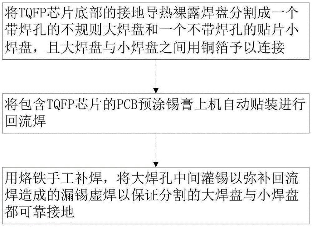
[0013] Please refer to figure 1 , the present invention provides a kind of PCB encapsulation design and soldering method of a TQFP chip, comprising the following steps:

[0014] Divide the ground heat conduction exposed pad at the bottom of the TQFP chip into an irregular large pad with a solder hole and a small patch pad without a solder hole, and connect the large pad and the small pad with copper foil ;

[0015] Automatically mount the PCB pre-coated solder paste containing the TQFP chip on the machine for reflow soldering;

[0016] Use a soldering iron to manually repair the soldering, and fill the middle of the large soldering hole with tin to make up for the solder leakage caused by reflow soldering, so as to ensure that the divided large pads and small pads are reliably grounded.

[0017] The defective ...


PUM


Abstract

The invention provides a PCB packaging design and welding method of a TQFP chip. The PCB packaging design and welding method comprises the steps of dividing a grounded heat conducting exposed welding plate at the bottom of the TQFP chip into a big irregular welding plate with a welding hole, and a small SMT welding plate without welding holes, and connecting the big welding plate and the small welding plate with copper foil; loading PCB pre-coating solder paste containing the TQFP chip for automatic sticking and mounting, and carrying out reflow soldering; and finally, manually repairing welding through using soldering iron, and filling the middle part of the large welding hole with tin to make up the tin leaking and insufficient solder caused by reflow soldering, so as to guarantee that the divided big welding plate and the small welding plate are reliably grounded. The welding fraction defective of the TQFP package chips, welded through the method, on a PCB, is obviously decreased, the production cost is reduced, and the product quality is improved.

Description

technical field [0001] The invention relates to the field of circuit board design and welding, in particular to a PCB package design and welding method of a TQFP chip. Background technique [0002] At present, electronic products on the market are becoming more and more complex, and the types of electronic components are becoming more and more abundant. There is a large thermally conductive exposed pad at the bottom of many chips, and generally this pad is GND, we call it E-PAD. It is an aspect of PCB design that is easily overlooked, and it is critical to achieve the best performance and effective heat dissipation of your PCB design. It is an important link through which all internal grounds of the chip are connected to other components of the circuit. Therefore, it is required that the E-PAD of this chip must be fully grounded. Once the grounding is unreliable, the chip cannot work normally. [0003] So the question is, how to design this kind of pad, and how to solder ...

Claims


Application Information

Patent Timeline
Patent Type & Authority Applications(China)
IPC IPC(8): B23K1/00B23K3/00
CPCB23K1/00B23K3/00
Inventor 邓丽何涛刘宝华
Owner 长沙奥托自动化技术有限公司
Why Eureka
Try Eureka