A cmos structure and its manufacturing method

A manufacturing method and device structure technology, applied in semiconductor/solid-state device manufacturing, semiconductor devices, electrical components, etc., to achieve low subthreshold slope and leakage current, improve device performance, and improve the effects of short channel effects

Active Publication Date: 2018-09-07
北京中科微投资管理有限责任公司
View PDF2 Cites 0 Cited by
  • Summary
  • Abstract
  • Description
  • Claims
  • Application Information

AI Technical Summary

Problems solved by technology

[0003] The present invention provides a new CMOS structure and its manufacturing method. On the basis of the existing technology, a new device structure is used, that is, a U-shaped channel FinFET is used as a transistor in CMOS, so that the gate length of the device is not affected by the footprint. Size limitation, effectively solve the problems caused by the short channel effect

Method used


Image

  • A cmos structure and its manufacturing method
  • A cmos structure and its manufacturing method
  • A cmos structure and its manufacturing method

Examples


Embodiment Construction

[0042] In order to make the objectives, technical solutions and advantages of the present invention clearer, the embodiments of the present invention will be described in detail below with reference to the accompanying drawings.

[0043] The following describes in detail the embodiments of the present invention, examples of which are illustrated in the accompanying drawings, wherein the same or similar reference numerals refer to the same or similar elements or elements having the same or similar functions throughout. The embodiments described below with reference to the accompanying drawings are exemplary and are only used to explain the present invention, but not to be construed as a limitation of the present invention.

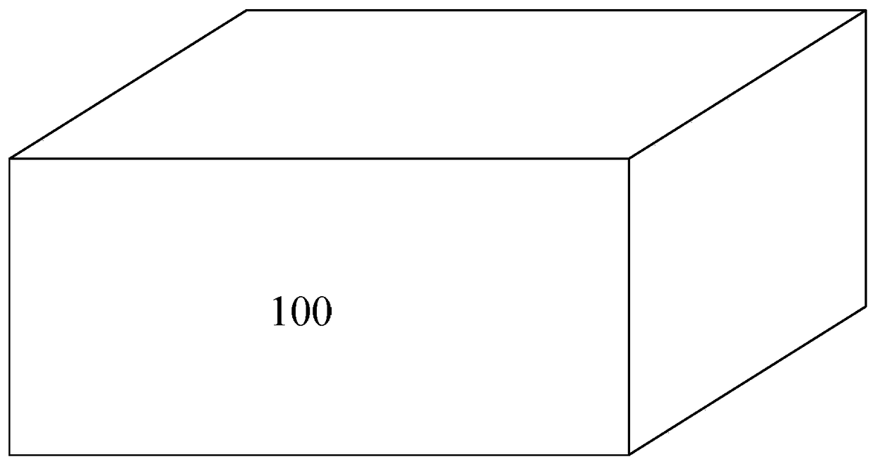
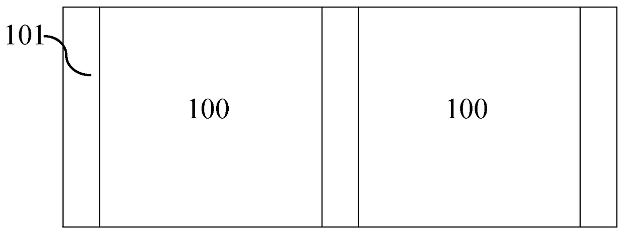
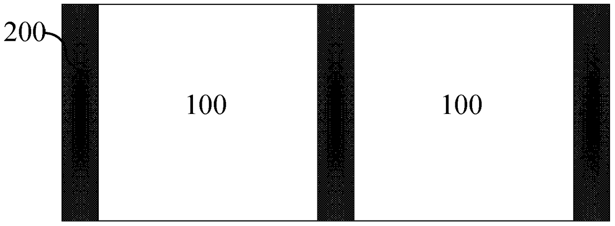
[0044] like Figure 11 As shown, the present invention provides a FinFET structure, including: a substrate 100, in order to be well compatible with existing processes, the substrate 100 adopts but is not limited to using a silicon substrate; a device isolat...


PUM


Abstract

The invention provides a CMOS structure and a manufacturing method thereof. The CMOS structure comprises a substrate, a device isolation region, a gate laminate and an isolation region. The device isolation region divides the substrate into a first region and a second region. The first region contains a first fin and a second fin. A first source region and a first drain region are respectively located at top regions of the first and second fins to constitute an NMOS structure with a U-shaped channel. The second region contains a third fin and a fourth fin. A second source region and a second drain region are respectively located at top regions of the third and fourth fins to constitute a PMOS structure with a U-shaped channel. The invention provides a novel device structure based on the existing FinFET technology, the gate length of a device is no longer limited by the footprint size, and the problem brought by a short channel effect is effectively solved.

Description

technical field [0001] The present invention relates to a method for manufacturing a semiconductor device, in particular, to a method for manufacturing a CMOS. technical background [0002] Moore's Law states that the number of transistors that can be accommodated on an integrated circuit doubles every 18 months, and the performance doubles at the same time. At present, with the development of integrated circuit technology and technology, diodes, MOSFETs, FinFETs and other devices have appeared successively, and the node size has been continuously reduced. However, since 2011, silicon transistors have approached the atomic level and reached the physical limit. Due to the natural properties of this substance, in addition to the short channel effect, the quantum effect of the device also has a great impact on the performance of the device. Breakthroughs in the speed and performance of silicon transistors are hard to come by. Therefore, how to greatly improve the performance ...

Claims


Application Information

Patent Timeline
Patent Type & Authority Patents(China)
IPC IPC(8): H01L29/78H01L29/06H01L21/336H01L21/8238H01L21/762
Inventor 李睿刘云飞尹海洲
Owner 北京中科微投资管理有限责任公司
Why Eureka
Try Eureka