

Touch panel and touch display module
A touch panel and cover technology, applied in the fields of optics, instruments, electrical digital data processing, etc., can solve the problems of expensive ITO production cost, high equipment cost, large surface resistance of ITO, etc., and achieve the elimination of grid line outline and Murray ripple problem, improved visual effects, and reduced reflectivity
- Summary
- Abstract
- Description
- Claims
- Application Information
AI Technical Summary
Problems solved by technology
Method used
Image

Examples
Embodiment Construction
[0054] In order to make the purpose, technical solutions and advantages of the present invention more clear, the present invention will be further described in detail below in conjunction with the accompanying drawings and implementation examples. It should be understood that the specific embodiments described here are only used to explain the present invention, not to limit the present invention.
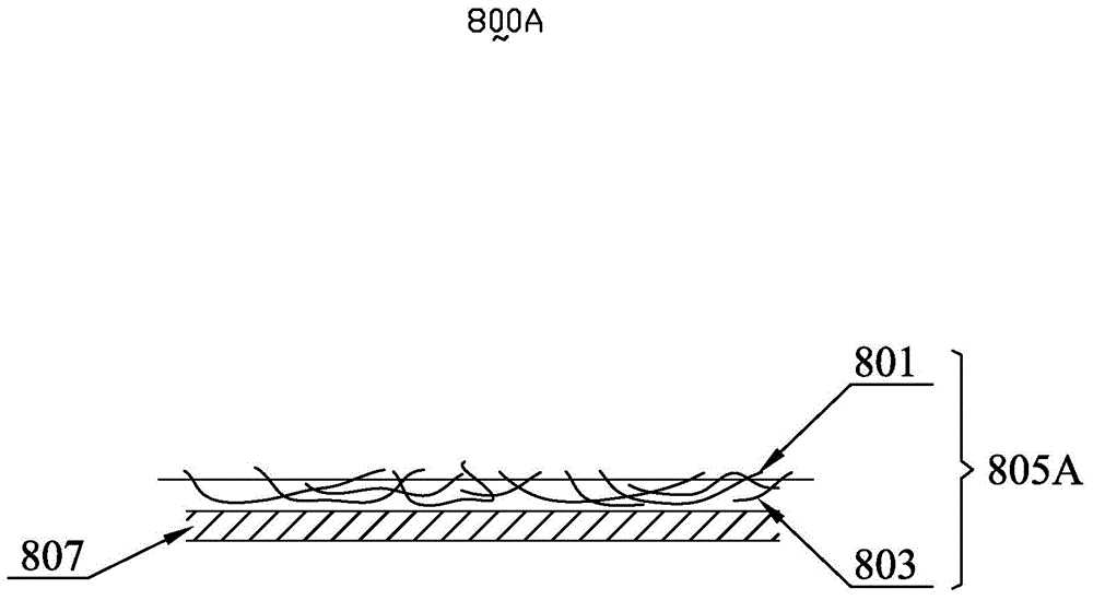
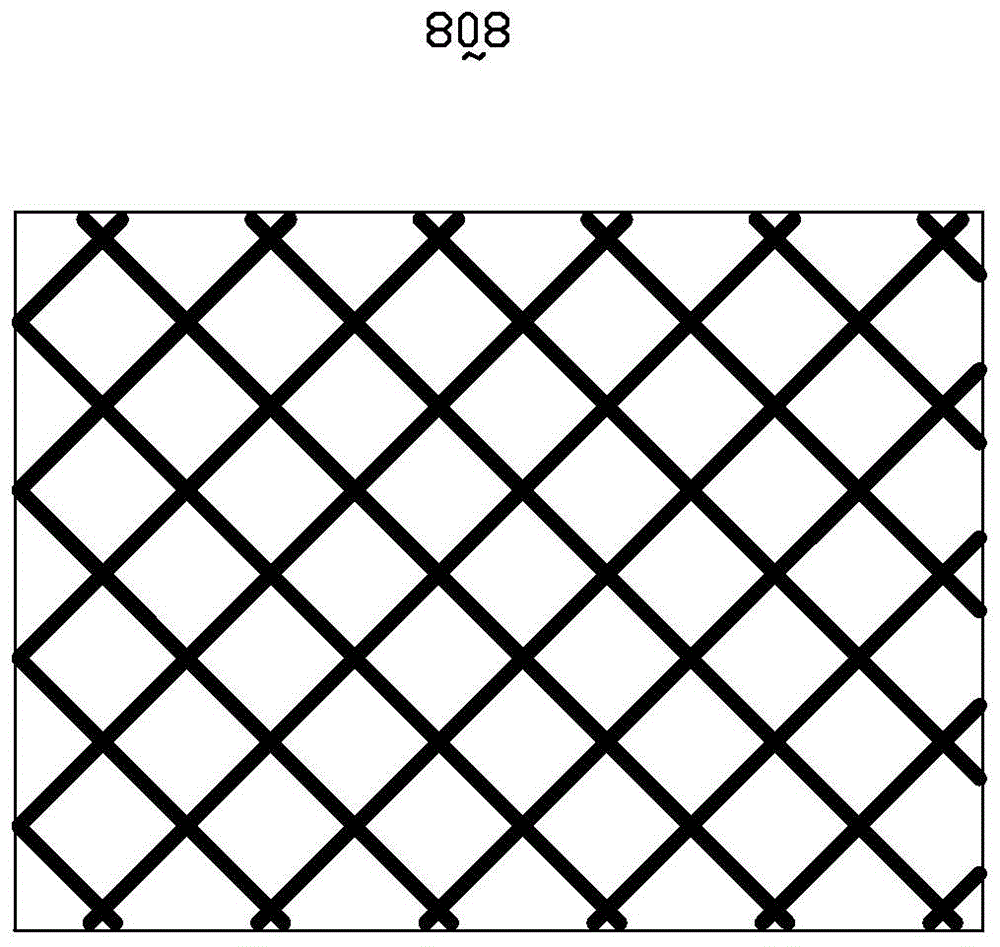
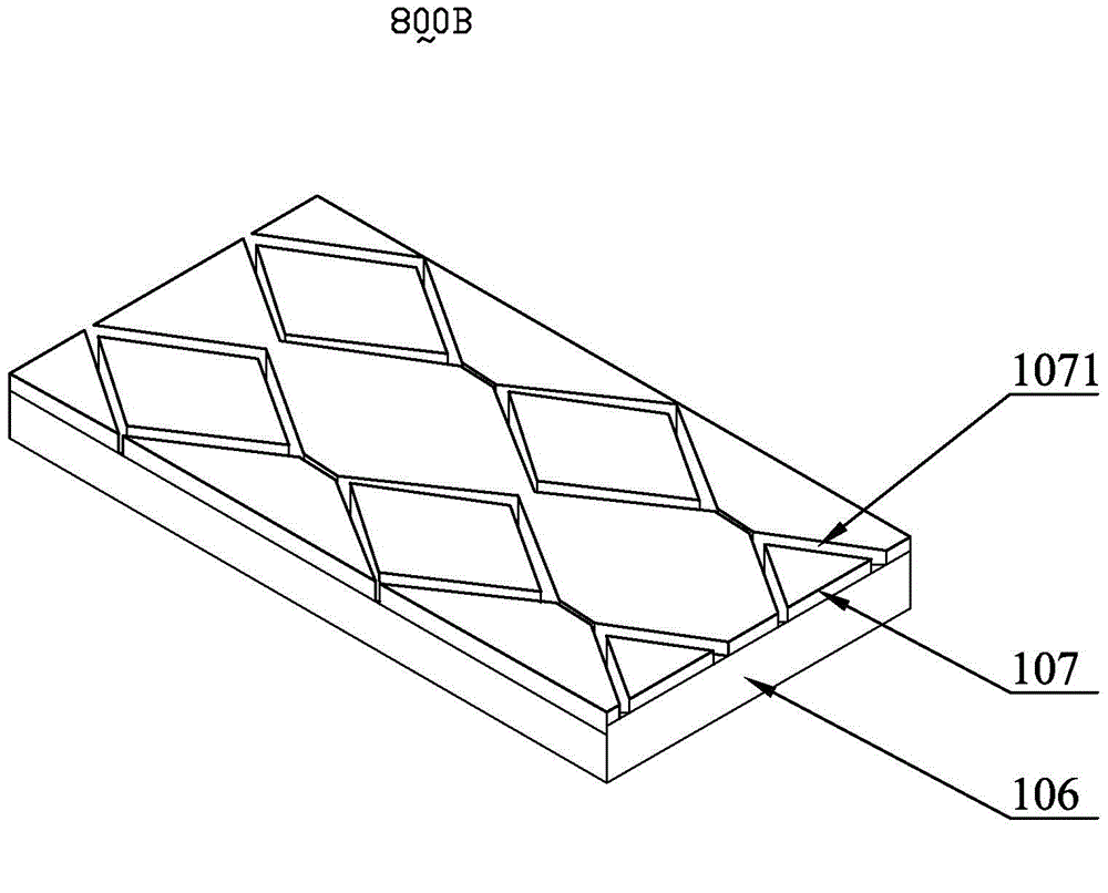
[0055] see Figure 1A , 1B with 2A, 2B, Figure 1A It is a schematic diagram of a cut-away structure of a silver nano wire conductive film 800A. The transparent conductive coating 805A is a coating of nano silver paint on the upper surface of a substrate 807, and the paint includes a matrix 803 or a plurality of nano silver wires embedded in the matrix 803 801. Subsequently, the transparent conductive coating 805A can be patterned (for example, using exposure and development technology) to form a nano-silver conductive grid 808, such as Figure 1B shown; Figure 2A It is a three-...
PUM
 Abstract
Description
Claims
Application Information