Traceable chip, manufacturing method thereof and electronic device

A traceable and chip-based technology, applied to electrical components, electrostatic transducers, microphones, sensors, etc., can solve problems such as the inability to identify and track chips, and achieve the effect of improving the manufacturing process

Inactive Publication Date: 2016-03-23
GOERTEK INC
View PDF3 Cites 2 Cited by
  • Summary
  • Abstract
  • Description
  • Claims
  • Application Information

AI Technical Summary

Problems solved by technology

[0004] In view of this, the present invention provides a traceable chip and its manufacturing method and electronic equipment to solve the problem that the packaged chip cannot be identified and tracked in the prior art

Method used


Image

  • Traceable chip, manufacturing method thereof and electronic device
  • Traceable chip, manufacturing method thereof and electronic device
  • Traceable chip, manufacturing method thereof and electronic device

Examples


Embodiment Construction

[0044] The following will clearly and completely describe the technical solutions in the embodiments of the present invention with reference to the accompanying drawings in the embodiments of the present invention. Obviously, the described embodiments are only some, not all, embodiments of the present invention. Based on the embodiments of the present invention, all other embodiments obtained by persons of ordinary skill in the art without making creative efforts belong to the protection scope of the present invention.

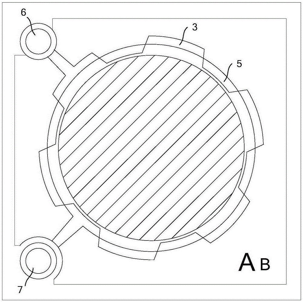
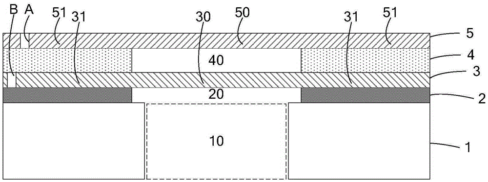
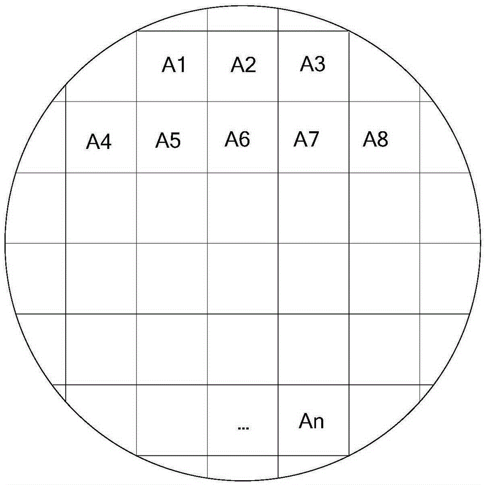
[0045] An embodiment of the present invention provides a traceable chip, the traceable chip has a first mark and a second mark on the structural layer; the first mark is used to mark the exposure area of ​​the chip on the silicon wafer, The silicon wafer has a plurality of exposure areas, and the first marks of the chips in the same exposure area are the same, and the first marks of the chips in different exposure areas are different; the second mark is used to...


PUM


Abstract

The invention provides a traceable chip, a manufacturing method thereof and an electronic device. The chip is provided with a first identifier and a second identifier; the first identifier is used for identifying an exposure area of the chip on a silicon wafer, the silicon wafer is provided with a plurality of exposure areas, the first identifiers of the chips in the same exposure area are the same, and the first identifiers of the chips in different exposure areas are different; the second identifier is used for identifying the position information of the chip in the corresponding exposure area, wherein the second identifiers of different chips in the same exposure area are different, so that the position of the chip on the silicon wafer can be determined according to the first identifier and the second identifier, and then flaw information of the area corresponding to the chip on the silicon wafer can be obtained according to the performance parameter of the packaged chip, and in this way, the manufacturing process can be improved in a subsequent manufacturing process to avoid the problem that the flaws of the silicon wafer influence the performance of the chip.

Description

technical field [0001] The invention relates to the technical field of semiconductor manufacturing, and more specifically relates to a traceable chip, its manufacturing method and electronic equipment. Background technique [0002] The MEMS microphone chip is a microphone chip manufactured based on MEMS (Micro-Electro-Mechanical System, Micro-Electro-Mechanical System) technology. Since the MEMS microphone chip has the advantages of small package size, high reliability, and low cost, it has been widely used in various electronic devices with voice functions such as mobile phones, tablet computers, and monitoring devices. [0003] The existing MEMS microphone chip manufacturing method is to first manufacture a plurality of chips on a silicon wafer, and then cut and package the chips to form individual MEMS microphone chips. However, since the appearance of each packaged MEMS microphone chip is the same, it is impossible for people to identify and track the packaged MEMS micr...

Claims


Application Information

Patent Timeline
Patent Type & Authority Applications(China)
IPC IPC(8): H04R19/04H04R31/00
CPCH04R19/04H04R31/00H04R2201/003
Inventor 蔡孟锦田昕郑成龙王景雪李江龙
Owner GOERTEK INC
Why Eureka
Try Eureka