Metal oxide semiconductor field effect transistor on-resistance measuring method

An oxide semiconductor and on-resistance technology, which is used in the testing of single semiconductor devices, measuring devices, measuring electrical variables, etc., and can solve problems such as inability to achieve Kelvin connection, unstable testing, and inaccurate test values.

Active Publication Date: 2016-03-30
华润赛美科微电子(深圳)有限公司
View PDF6 Cites 12 Cited by
  • Summary
  • Abstract
  • Description
  • Claims
  • Application Information

AI Technical Summary

Problems solved by technology

[0004] However, due to the structural limitations of the wafer, there are only two PADs on the front of the actual wafer, the gate and the source, and the drain is on the back of the wafer.
Since the entire wafer is adsorbed on the chuck of the probe station during the test, and the back of the wafer is

Method used


Image

  • Metal oxide semiconductor field effect transistor on-resistance measuring method
  • Metal oxide semiconductor field effect transistor on-resistance measuring method
  • Metal oxide semiconductor field effect transistor on-resistance measuring method

Examples


Embodiment Construction

[0015] In order to make the objects, features and advantages of the present invention more comprehensible, specific implementations of the present invention will be described in detail below in conjunction with the accompanying drawings.

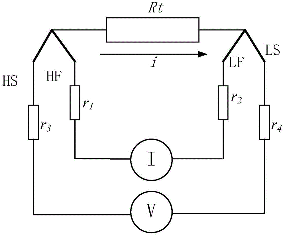
[0016] figure 1 It is a circuit schematic diagram of a typical Kelvin test method connecting test resistors. For each test point, there is an excitation line F and a detection line S. For measuring the resistance at both ends, it is a high-potential excitation line HF and a low-potential excitation line. Line LF, a high potential detection line HS, and a low potential detection line LS. The excitation lines (high potential excitation line HF and low potential excitation line LF) are used to transmit current, and the detection lines (high potential detection line HS and low potential detection line LS) monitor the voltage of the test point. The two are strictly separated and each constitutes an independent circuit. At the same time, it is r...


PUM


Abstract

The invention relates to a metal oxide semiconductor field effect transistor on-resistance measuring method which comprises the following steps: sucking the back surface of a wafer through a chuck; connecting a low-potential excitation line and a low-potential detection line in a Kelvin test method to a source electrode of a MOS transistor to be tested, connecting a first high-potential excitation line and a first high-potential detection line in the Kelvin test method to a grid electrode of the MOS transistor to be tested, selecting another MOS transistor on the wafer as an auxiliary transistor, connecting a second high-potential excitation line in the Kelvin test method to the chuck, and connecting a second high-potential detection line in the Kelvin test method to a source electrode of the auxiliary transistor; and adding a break-over voltage between a grid electrode and the source electrode of the auxiliary transistor to enable the auxiliary transistor to be in an on state, powering on an on-resistance measuring circuit and measuring the on-resistance of the MOS transistor to be tested. Through a die compensation method, real Kelvin connection is realized, so that on-resistance of the MOS transistor can be measured stably and accurately.

Description

technical field [0001] The invention relates to the measurement of resistance, in particular to a method for measuring the on-resistance of metal oxide semiconductor field effect transistors. Background technique [0002] Power control and power conversion is an important field where metal oxide semiconductor field effect transistors (MOSFETs, MOS tubes for short) are widely used. In such applications, MOS tubes are usually used as switches, and on-resistance is one of the most critical parameters. , which directly affects the stability of the application circuit. Therefore, the on-resistance (R dson ) Accurate measurement has become the focus of MOS tube testing. [0003] With the continuous introduction of new MOSFETs, the resistance value of the on-resistance is getting smaller and smaller, and products on the order of milliohms are already common. In order to accurately measure the tiny conduction resistance, the Kelvin method is usually used for resistance testing. ...

Claims


Application Information

Patent Timeline
IPC IPC(8): G01R31/26G01R27/02
Inventor 顾汉玉
Owner 华润赛美科微电子(深圳)有限公司
Why Eureka
Try Eureka