

Array substrate, display panel and display device
A technology for array substrates and display panels, applied in the fields of array substrates, display panels, and display devices, can solve problems affecting display quality, slow response speed of liquid crystal molecules, and image smearing, so as to improve image smearing and display quality Effect
- Summary
- Abstract
- Description
- Claims
- Application Information
AI Technical Summary
Problems solved by technology
Method used
Image

Examples
Embodiment 1
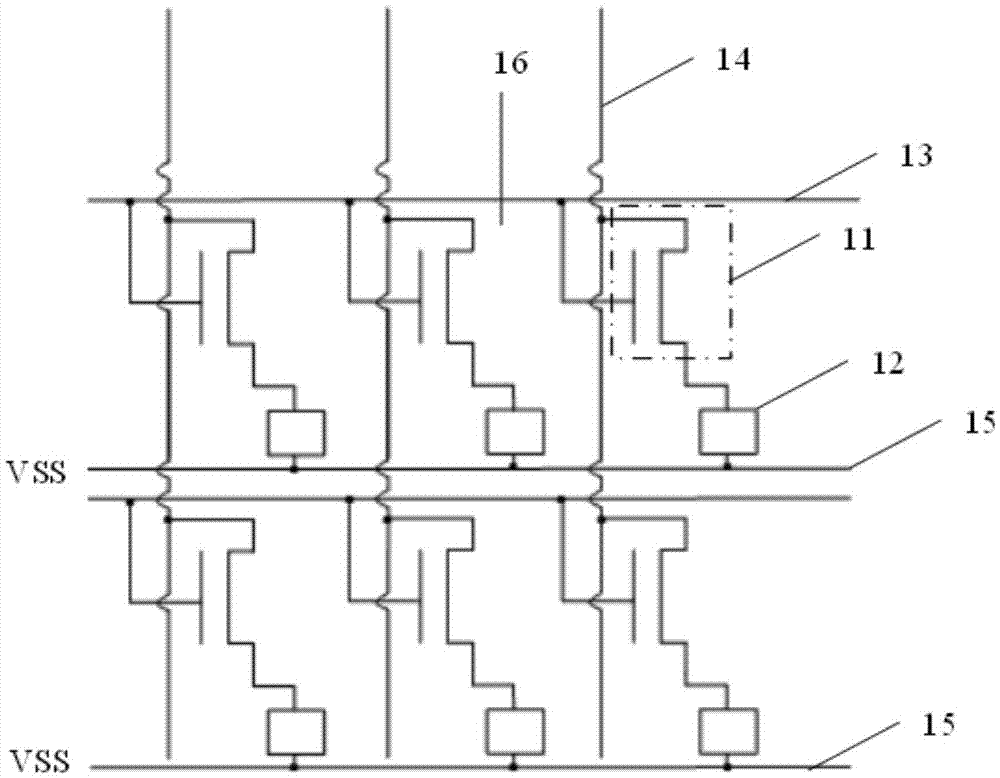
[0039] An array substrate such as figure 1 As shown, it includes a plurality of pixel units 16 formed by vertical crossing of gate lines 13 and data lines 14 on a base substrate (not shown in the figure), and each pixel unit 16 includes a light switch function to control the opening and closing of the pixel. The switching transistor 11 also includes a thermo-optical switch 12 with a thermally induced refractive index change;
[0040] It should be noted, figure 1 It is only a schematic description that the pixel unit includes a thermo-optic switch, and the relative size of the thermo-optic switch and the pixel unit is not described.
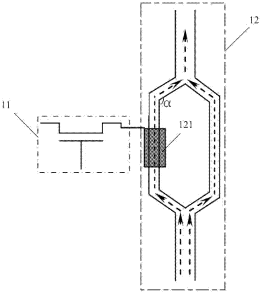
[0041] In order to explain more clearly, the setting method of thermo-optic switch in each pixel unit, such as Picture 8 As shown, it is a partial enlarged schematic diagram of the pixel unit. In practical application scenarios, the thermo-optical switch 12 is disposed in the pixel unit and occupies almost the entire pixel unit, which can ensure that ...
Embodiment 2
[0069] This embodiment provides a display panel, in which an array substrate in the display panel can realize the display of different color gray scales through cooperation with a color filter substrate.
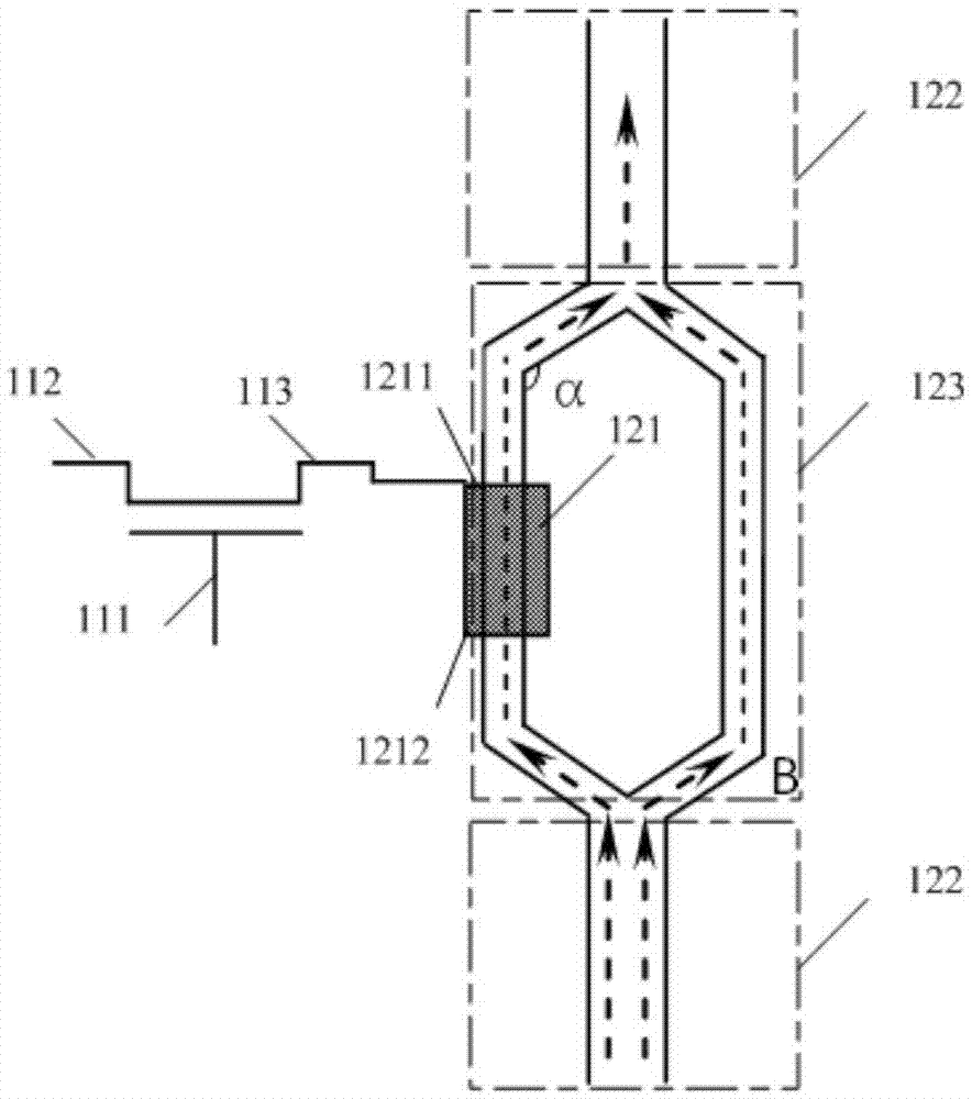
[0070] Optionally, the thermo-optical switch in each pixel unit covers the entire pixel unit area to avoid light leakage.
[0071] The color filter substrate can be a commonly used color filter substrate, and a black matrix can be arranged on the color filter substrate to further avoid light leakage.
[0072] The display panel includes an array substrate and a color filter substrate. The array substrate adopts the above-mentioned array substrate. The array substrate and the color filter substrate are combined to form, and the array substrate is composed of M×N pixel units.
[0073] In this embodiment, the array substrate and the pixel unit of the color filter substrate are in one-to-one correspondence, and each pixel unit is provided with a pixel unit; the red, green, and blue pixel ...
Embodiment 3
[0077] This embodiment provides a display device, which can achieve a flat panel display effect similar to a liquid crystal display device, and has high brightness and good contrast.
[0078] Such as Figure 7 As shown, a display device includes a backlight source 3 and a display panel. The display panel is the display panel in Embodiment 2, and the array substrate 1 is located between the backlight source 3 and the color filter substrate 2. Here, the backlight source 3 may be the backlight source 3 used in the existing LCD display device, or may be another structure capable of generating uniform light, which is not limited here.
[0079] In this embodiment, the direction of the end of the optical waveguide in the thermo-optical switch is in the same plane as the propagation direction of the light in the backlight, that is, the entire plane formed by the thermo-optical switch and the array substrate is in a vertical relationship.
[0080] The color filter substrate 2 is placed in fro...
PUM
 Abstract
Description
Claims
Application Information