Manufacturing method of semiconductor structure

A manufacturing method and semiconductor technology, applied in semiconductor/solid-state device manufacturing, electrical components, circuits, etc., can solve problems such as inability to absorb, wafer warping, falling and breaking, etc., to improve production yield and reduce The effect of changing the value and preventing warping

Inactive Publication Date: 2016-03-30
SEMICON MFG INT (SHANGHAI) CORP
View PDF6 Cites 0 Cited by
  • Summary
  • Abstract
  • Description
  • Claims
  • Application Information

AI Technical Summary

Problems solved by technology

[0004] The adverse effects of wafer warping and deformation are mainly manifested in: affecting the accuracy of lithography, it is difficult for the wafer to be loaded into the subsequent machine; during the process of machine loading and transmission, it cannot be adsorbed, resulting in falling and breaking; the wafer is seriously warped resulting in excessive internal stress and cracking of the wafer
These unfavorable factors can easily lead to the scrapping of the wafer in the subsequent semiconductor manufacturing process; in addition, the severe warpage of the wafer will also affect the packaging of the wafer
[0005] All in all, the warpage of the wafer brings considerable difficulties to the production of semiconductor integrated circuits, which seriously affects the product yield. Finding a simple and effective method to eliminate the warpage of the wafer is one of the problems that need to be solved urgently

Method used


Image

  • Manufacturing method of semiconductor structure
  • Manufacturing method of semiconductor structure
  • Manufacturing method of semiconductor structure

Examples


Embodiment Construction

[0035] It can be seen from the background art that how to eliminate wafer warpage is one of the current problems that need to be solved urgently.

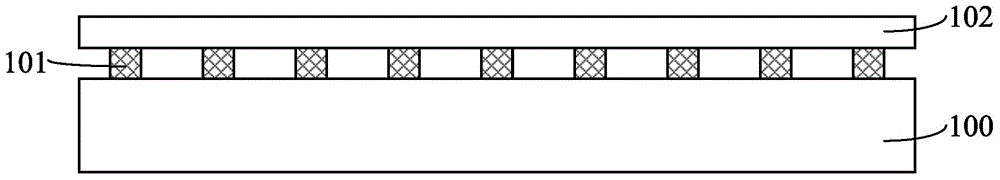
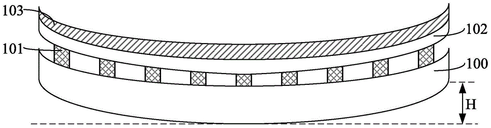
[0036] For research on the fabrication method of semiconductor structures, please refer to figure 1 , provide a support plate 100, bond the support plate 100 and the base 102 through the adhesive layer 101, the support plate 100 improves the mechanical strength of the base 102; please refer to figure 2 , the metal layer 103 is formed on the surface of the base 102. After the metal layer 103 is formed, the support plate 100, the base 102, and the metal layer 103 all warp and deform, and the warpage of the support plate 100, the base 102, and the metal layer 103 ( bow) is H, and the warpage H is the distance between the highest point of the support plate 100 and the line connecting the bottom edge of the support plate 100 .

[0037] After research, it was found that the main reason for the warpage and deformation of the substrate ...


PUM


Abstract

The invention discloses a manufacturing method of a semiconductor structure. The manufacturing method comprise the steps of: providing a substrate; forming a metal layer on the surface of the substrate; providing an annealing chamber; placing the metal layer in the annealing chamber for annealing treatment, wherein the temperature inside the annealing chamber during the process of annealing treatment is a first temperature; carrying out temperature decreasing treatment on the annealing chamber in which the metal layer is placed after the annealing treatment, so that the temperature inside the annealing chamber is decreased from the first temperature to a second temperature; and taking the substrate with the metal layer out from the annealing chamber with the second temperature. The manufacturing method reduces the temperature difference between the metal layer and the substrate when taking the substrate and the metal layer out from the annealing chamber, prevents the metal layer and the substrate from warping due to sudden temperature change, and increases production yield rate of the semiconductor structure.

Description

technical field [0001] The invention relates to the technology in the field of semiconductor manufacturing, in particular to a method for manufacturing a semiconductor structure. Background technique [0002] Usually wafer (wafer) refers to the silicon wafer used in the production of silicon semiconductor integrated circuits. Because its shape is mostly round, it is called a wafer; it can be processed into various circuit component structures on the wafer to make IC (Integrated Circuit) products with specific electrical functions. [0003] With the continuous progress of the semiconductor industry, the size of the wafer is getting larger and larger, and the structure of the components and devices formed on the basis of the wafer is becoming more and more complex, so a series of technical problems have arisen. Among them, wafer warpage is a very common problem, that is, the wafer is deformed. Generally, the overall shape of the wafer can be described by "warpage degree". The...

Claims


Application Information

Patent Timeline
Patent Type & Authority Applications(China)
IPC IPC(8): H01L21/02
Inventor 陈怡骏游宽结侯元琨
Owner SEMICON MFG INT (SHANGHAI) CORP
Why Eureka
Try Eureka