Semiconductor device forming method

A semiconductor and device technology, applied in the field of semiconductor device formation, can solve the problems that the electrical properties of semiconductor devices need to be improved, and achieve the effect of improving carrier mobility and stress effect

Active Publication Date: 2016-03-30
SEMICON MFG INT (SHANGHAI) CORP
View PDF3 Cites 16 Cited by
  • Summary
  • Abstract
  • Description
  • Claims
  • Application Information

AI Technical Summary

Problems solved by technology

[0005] The application of embedded silicon germanium and embedded carbon silicon technology can improve the carrier mobility of semiconductor devices, but in practical applications, it is found that there are still problems to be solved in the manufacturing process of semiconductor devices, and the electrical performance of semiconductor devices needs to be improved

Method used


Image

  • Semiconductor device forming method
  • Semiconductor device forming method
  • Semiconductor device forming method

Examples


Embodiment Construction

[0033] It can be seen from the background art that the electrical performance of semiconductor devices formed in the prior art needs to be improved.

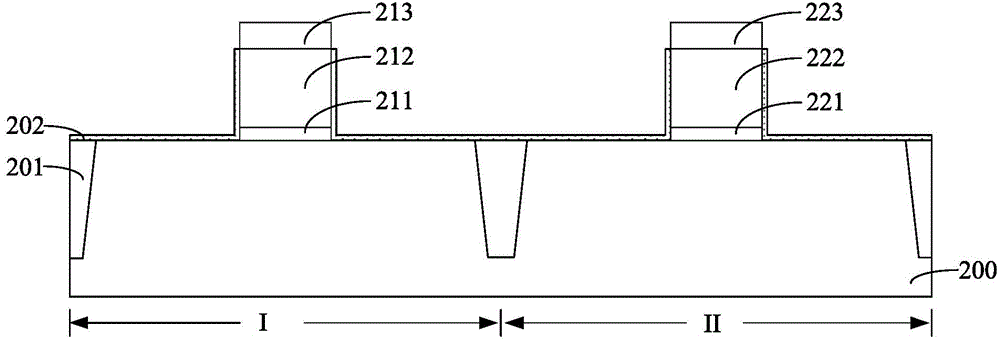
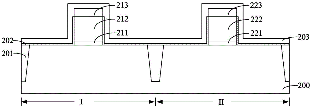
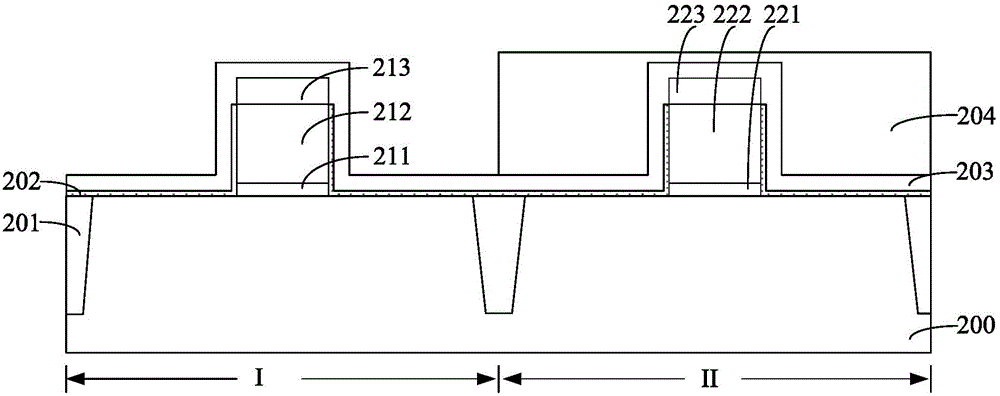
[0034] The formation process of the semiconductor device is studied. The formation process of the semiconductor device includes the following steps: step S101, providing a substrate including a first region and a second region, the substrate surface of the first region has a first gate structure, and the second region The surface of the substrate has a second gate structure; step S102, forming a first lightly doped region in the substrate on both sides of the first gate structure, forming a first lightly doped region in the substrate on both sides of the second gate structure The second lightly doped region; step S103, forming a first offset sidewall on the sidewall of the first gate structure, and forming a second offset sidewall on the sidewall of the second gate structure; step S104, forming The first mask layer covering the ...


PUM


Abstract

The invention discloses a semiconductor device forming method, and the method comprises the steps: providing a substrate, forming a first grid structure and a second grid structure on the surface of the substrate, and forming first mask layers on the surface of the substrate, the surface of the first grid structure and the surface of the second grid structure; Etching the parts, at two sides of the first grid structure, of the substrate to form a first groove, and forming a first offset side wall through the remaining first mask layer in a first region; forming a light-doped region in the substrate below the first offset side wall; forming a first stress layer which is filled in the first groove; forming a second mask layer; etching the parts, at two sides of the second grid structure, of the substrate to form a second groove, and forming a second offset side wall through the remaining first and second mask layers in a second region; forming a second light-doped region in the substrate below the second offset side wall; and forming a second stress layer filled in the second groove. The method effectively alleviates the hot carrier effect while improving the carrier mobility of a semiconductor device, and optimizes the electrical performances of the semiconductor device.

Description

technical field [0001] The invention relates to the technology in the field of semiconductor manufacturing, in particular to a method for forming a semiconductor device. Background technique [0002] With the continuous development of semiconductor technology, carrier mobility enhancement technology has been widely studied and applied. Improving the carrier mobility in the channel region can increase the driving current of MOS devices and improve the performance of the devices. [0003] In the existing manufacturing process of semiconductor devices, since stress can change the energy gap and carrier mobility of silicon materials, it has become more and more common means to improve the performance of semiconductor devices through stress. Specifically, by properly controlling the stress, the mobility of carriers (electrons in NMOS devices, holes in PMOS devices) can be increased, thereby increasing the driving current, so as to greatly improve the performance of semiconductor ...

Claims


Application Information

Patent Timeline
Patent Type & Authority Applications(China)
IPC IPC(8): H01L21/266
Inventor 虞肖鹏丁士成
Owner SEMICON MFG INT (SHANGHAI) CORP
Why Eureka
Try Eureka