Shield grid groove type MOSFET process method

A process method and trench-type technology, applied in electrical components, semiconductor/solid-state device manufacturing, circuits, etc., can solve problems such as high gate leakage, poor quality of oxide film between polysilicon, and the thickness of oxide film between polysilicon cannot be controlled separately

Inactive Publication Date: 2016-03-30
SHANGHAI HUAHONG GRACE SEMICON MFG CORP
View PDF3 Cites 9 Cited by
  • Summary
  • Abstract
  • Description
  • Claims
  • Application Information

AI Technical Summary

Problems solved by technology

[0003] This process method grows the inter-polysilicon oxide film and the gate oxide layer at the same time, the thickness of the inter-polysilicon oxide film cannot be controlled independe...

Method used


Image

  • Shield grid groove type MOSFET process method
  • Shield grid groove type MOSFET process method
  • Shield grid groove type MOSFET process method

Examples


Embodiment Construction

[0027] The shielded gate trench MOSFET process method of the present invention comprises the following process steps:

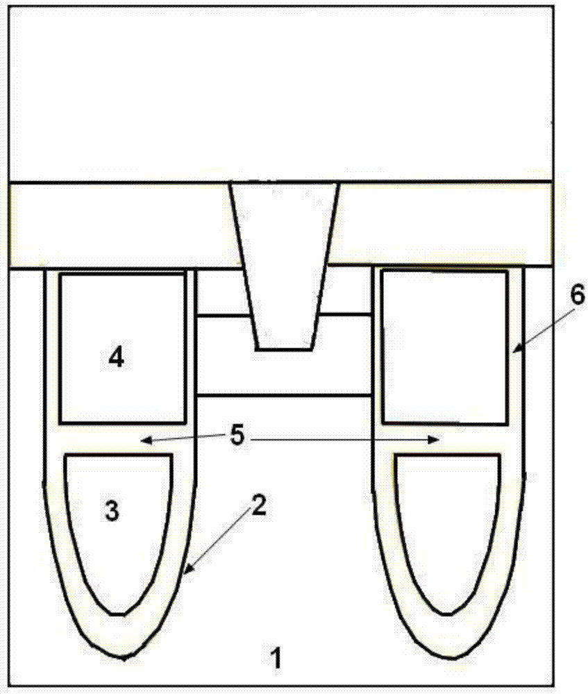
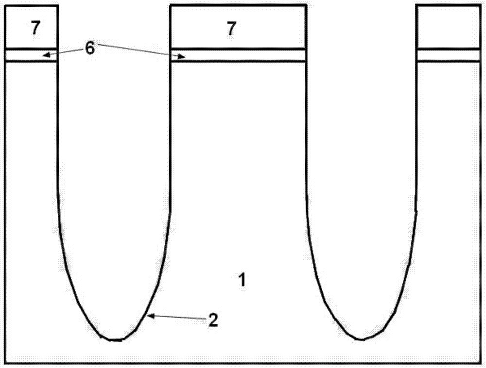
[0028] Step one, such as image 3 As shown, a layer of silicon oxide 6 is deposited on the silicon substrate 1, and then a layer of silicon nitride 7 is deposited. The photoresist defines a trench region on the silicon nitride and silicon oxide, and the photoresist is removed. Using silicon nitride and silicon oxide as hard masks, the substrate is etched to form trenches 2 .

[0029] Step 2, deposit a layer of silicon oxide 6 on the sidewall and bottom of the trench 2, such as Figure 4 shown.

[0030] Step three, such as Figure 5 As shown, the trench 2 is filled with polysilicon 3 and etched back, and the polysilicon is etched back until the surface is flush with the silicon oxide 6 on the substrate surface.

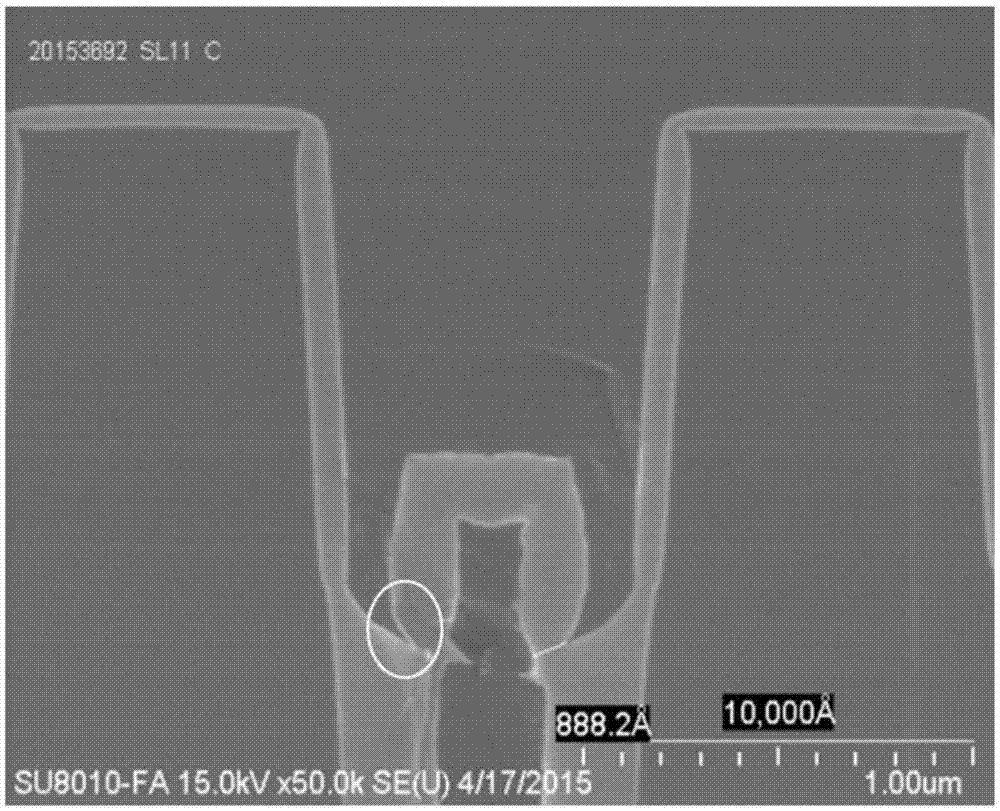
[0031] Step 4, etching back the polysilicon, and removing the silicon oxide 6 on the sidewall of the trench. The polysilicon is etched back unti...


PUM


Abstract

The invention discloses a shield grid groove type MOSFET process method, comprising: a first step, with silicon nitride and silicon oxide as a hard mask, etching a substrate to form a groove; a second step, depositing a layer of silicon oxide on the side wall and the bottom of the groove; a third step, filling polysilicon in the groove and etching back; a fourth step, etching back the polysilicon, and removing the silicon oxide on the side wall of the groove; a fifth step, depositing a layer of silicon nitride to cover the inner side wall of the groove and the polysilicon; a sixth step, etching the silicon nitride above the polysilicon to expose the polysilicon; a seventh step, depositing silicon oxide above the polysilicon; an eighth step, removing the silicon nitride on the entire device; a ninth step, depositing silicon oxide, depositing polysilicon and etching back to form a groove polysilicon grid; and a tenth step, forming a body region, injecting a source region, and depositing interlevel dielectric to form contact hole fabrication metal process. The process disclosed by the invention is used for realizing single control of oxide films and gate oxide between the polysilicon, and solving the problem of relatively high current leakage of the grid of the device.

Description

technical field [0001] The invention relates to the field of semiconductor integrated circuit manufacturing, in particular to a shielding gate trench type MOSFET process method. Background technique [0002] The structure of the shielded gate trench MOSFET is as follows figure 1 As shown, the trench is divided into upper and lower parts. The lower half of the trench is filled with polysilicon as the source, and the upper half of the trench is filled with polysilicon as the gate. The gate, source and trench are all separated by an oxide layer. The process method of this device is to first deposit a layer of oxide layer on the silicon substrate as a hard mask, then use photoresist to define the pattern of the hard mask, and then remove the photoresist, and use the pattern defined by the hard mask Etch the substrate to form a trench, then deposit an oxide layer, fill the trench with polysilicon, etch to form a source, then deposit a gate oxide layer, deposit polysilicon and et...

Claims


Application Information

Patent Timeline
IPC IPC(8): H01L21/336
CPCH01L29/66477
Inventor 丛茂杰
Owner SHANGHAI HUAHONG GRACE SEMICON MFG CORP
Why Eureka
Try Eureka