Terminal protection structure of super-junction device

A terminal protection structure and superjunction device technology, applied in semiconductor devices, electrical components, circuits, etc., can solve the problems of difficulty in process realization, poor device leakage, poor leakage characteristics, etc., to improve reliability and reduce movable ions. , the effect of improving the distribution of electric field strength

Active Publication Date: 2016-03-30
SHENZHEN SANRISE TECH CO LTD
View PDF9 Cites 14 Cited by
  • Summary
  • Abstract
  • Description
  • Claims
  • Application Information

AI Technical Summary

Problems solved by technology

[0008] like figure 1 As shown, in the terminal region, that is, in the 3rd region, the P-type pillar 203 and the N-type pillar 204 are ring structures connected end to end, and the P-type pillar 203 is generally filled with a P-type epitaxial layer after forming a trench in the N-type epitaxial layer. Silicon formation, in the trench filling process, the trench is prone to defects at the position of the bend (whether it is a right angle or a bend with a little curvature), and when there is a large electric field intensity in this area, the leakage characteristics are poor. With curved parts, there will be local charge balance, so that high breakdown voltage cannot be obtained, and the device leakage will be poor
In order to solve the problem of local charge balance, the existing technology is to carry out special design at the corner, such as adding small square P-pillars, but this is very difficult in process realization

Method used


Image

  • Terminal protection structure of super-junction device
  • Terminal protection structure of super-junction device
  • Terminal protection structure of super-junction device

Examples


Embodiment 1

[0055] Embodiment 1 of the present invention super junction device:

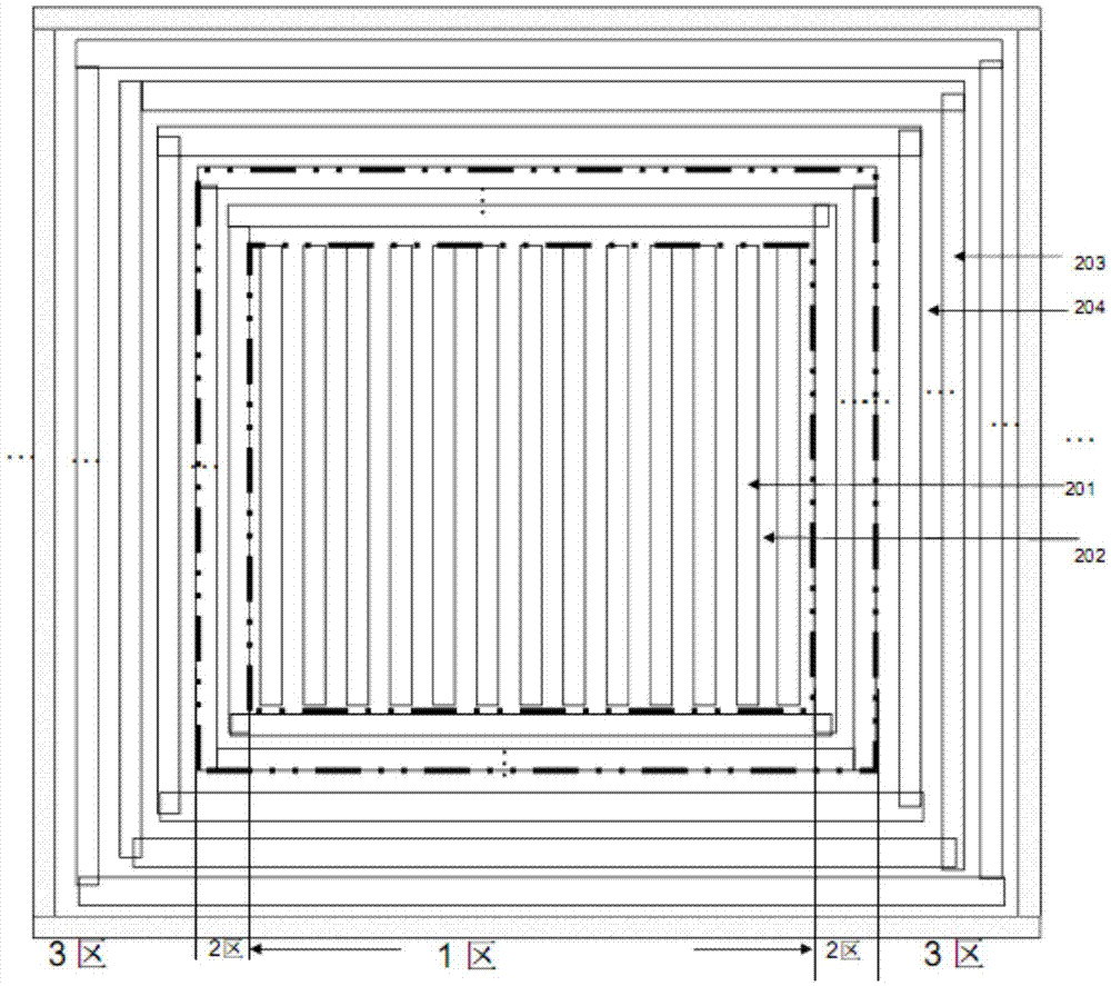
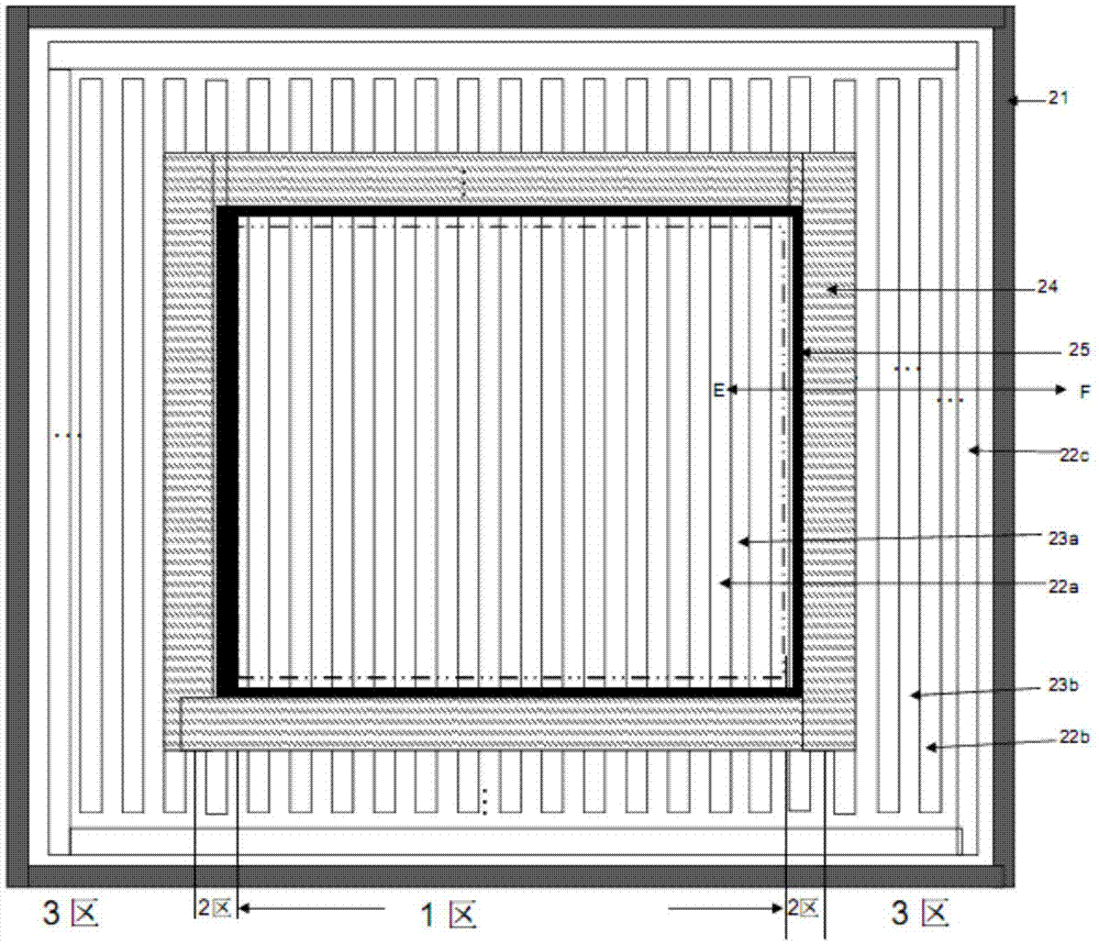
[0056] Such as figure 2 As shown, it is a top view of a super-junction device in an embodiment of the present invention; in the terminal protection structure of a super-junction device in an embodiment of the present invention, the super-junction device includes a charge flow region and a terminal protection structure, and the middle region of the super-junction device is a charge flow region , the terminal protection structure surrounds the periphery of the charge flow area, the terminal protection structure includes a transition area and a voltage bearing area, the transition area is located between the charge flow area and the voltage bearing area, figure 2 Zone 1 represents the charge flow zone, Zone 2 denotes the transition zone, and Zone 3 denotes the voltage bearing zone.

[0057] The current flow region includes a first partial super junction structure composed of alternately arranged first P-type...


PUM


Abstract

The invention discloses a terminal protection structure of a super-junction device. A P-type column and an N-type column of a super-junction structure of a current flow area are in a bar-shaped structure and are parallel to each other. A part of super-junction structure in the terminal protection structure is formed through extending the P-type column and the N-type column of the current flow area along a length direction. Another part of super-junction structure in the terminal protection structure is formed by alternatively arranging a second P-type column and a second N-type column of the bar-shaped structure, wherein the second P-type column and the second N-type column are parallel to the P-type column and the N-type column of the current flow area. A field plate and a P-type ring are formed in a transition area. A cut-off ring is formed on an outermost end of a voltage bearing area. The P-type column and the N-type column of the super structure of the terminal protection structure are in a long strip shape without turns. An electric leakage characteristic and reliability of the device can be increased and a smallest terminal size can be used to acquire a high breakdown voltage.

Description

technical field [0001] The invention relates to a semiconductor integrated circuit, in particular to a terminal protection structure of a superjunction device. Background technique [0002] The super junction structure is composed of alternately arranged N-type pillars and P-type pillars. If the superjunction structure is used to replace the N-type drift region in the vertical double-diffused MOS transistor (VerticalDouble-diffused Metal-Oxide-Semiconductor, VDMOS) device, the conduction path is provided through the N-type column in the conduction state, and the P-type The pillars do not provide a conduction path; in the cut-off state, the PN pillars bear the reverse bias voltage together, forming a super-junction metal-oxide-semiconductor field-effect transistor (Metal-Oxide-Semiconductor Field-Effect Transistor, MOSFET). The super-junction MOSFET can greatly reduce the on-resistance of the device by using a low-resistivity epitaxial layer when the reverse breakdown voltag...

Claims


Application Information

Patent Timeline
Patent Type & Authority Applications(China)
IPC IPC(8): H01L29/06H01L29/40
CPCH01L29/0634H01L29/0638H01L29/402
Inventor 肖胜安曾大杰
Owner SHENZHEN SANRISE TECH CO LTD
Why Eureka
Try Eureka