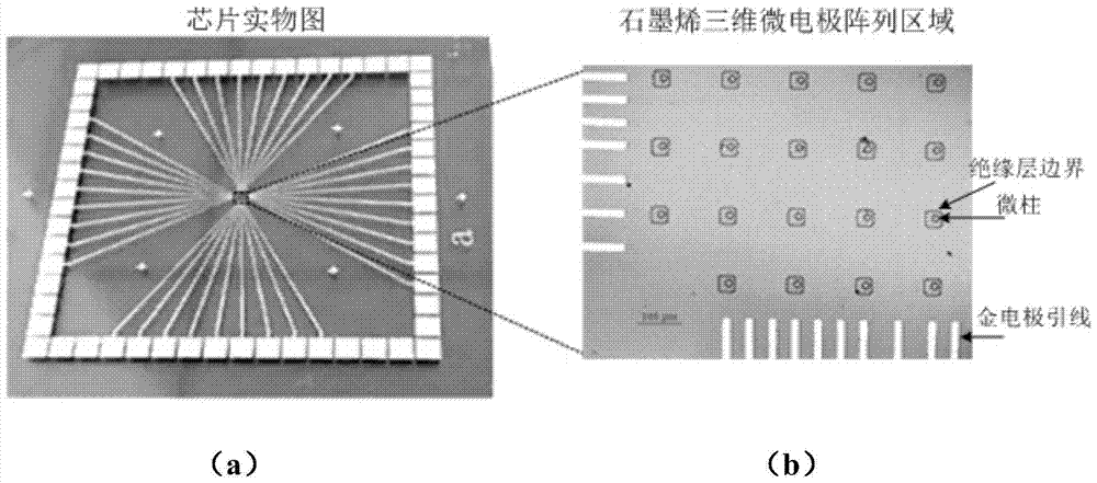
A graphene three-dimensional microelectrode array chip, method and application thereof
A graphene and micro-electrode technology, which is applied in the field of electrophysiological detection of cells and tissues, can solve the problems of flexible cells or tissues in close contact, increase the specific surface area of electrode sites, etc., and achieve excellent electrochemical stability and excellent electrical properties. Properties, the effect of high light transmittance
- Summary
- Abstract
- Description
- Claims
- Application Information
AI Technical Summary
Problems solved by technology
Method used
Image
Examples
Embodiment 1
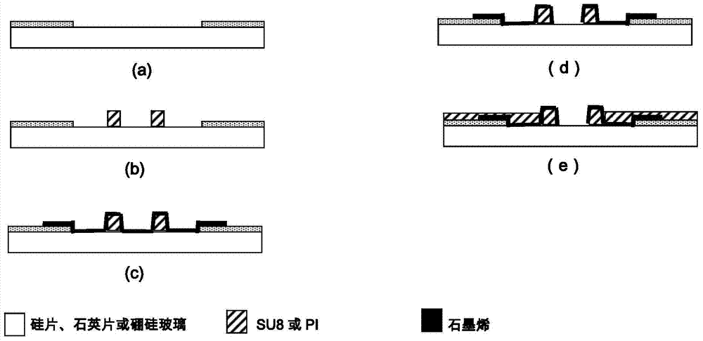
[0015] The manufacturing process of graphene three-dimensional microelectrode chip is as follows: figure 2 As shown, the details are as follows:
[0016] (1) Clean the substrate: use Phiranha solution to clean the silicon wafer or quartz wafer or borosilicate glass wafer (such as Prex7740), then rinse with deionized water, blow dry with nitrogen, and treat with oxygen plasma for 5 minutes;
[0017] (2) Lift-off process to make the outer electrode leads and pins in the outer microelectrode array area: Spin-coat AZ4620 on the substrate, pattern it by photolithography, then sputter the metal layer (titanium / gold), and remove the photolithography with acetone Glue, leaving the metal layer. ( figure 2 .a)
[0018] (3) Production of three-dimensional microcolumn arrays: Spin-coat negative photoresist (SU8 3005 for silicon wafers, PI 7510 for quartz wafers and Prex7740 borosilicate glass), control the speed at 3000r / min, and after photolithography and development, cure to form ...
Embodiment 2
[0023] Graphene three-dimensional microelectrode performance testing method
[0024] The electrochemical impedance and cyclic voltammetry curve test methods are as follows:
[0025] (1) Gamry reference 600 electrochemical workstation was used to perform electrochemical characterization of microelectrodes using a three-electrode system.
[0026] (2) A plastic cavity is glued on the substrate with PDMS, and the microelectrode array area is located in the cavity. Inject PBS solution into the cavity.
[0027] (3) The graphene three-dimensional microelectrode site is used as the working electrode, the Ag / AgCl is used as the reference electrode, and the platinum wire is used as the counter electrode, and the three electrodes are immersed in the PBS solution described in (2).
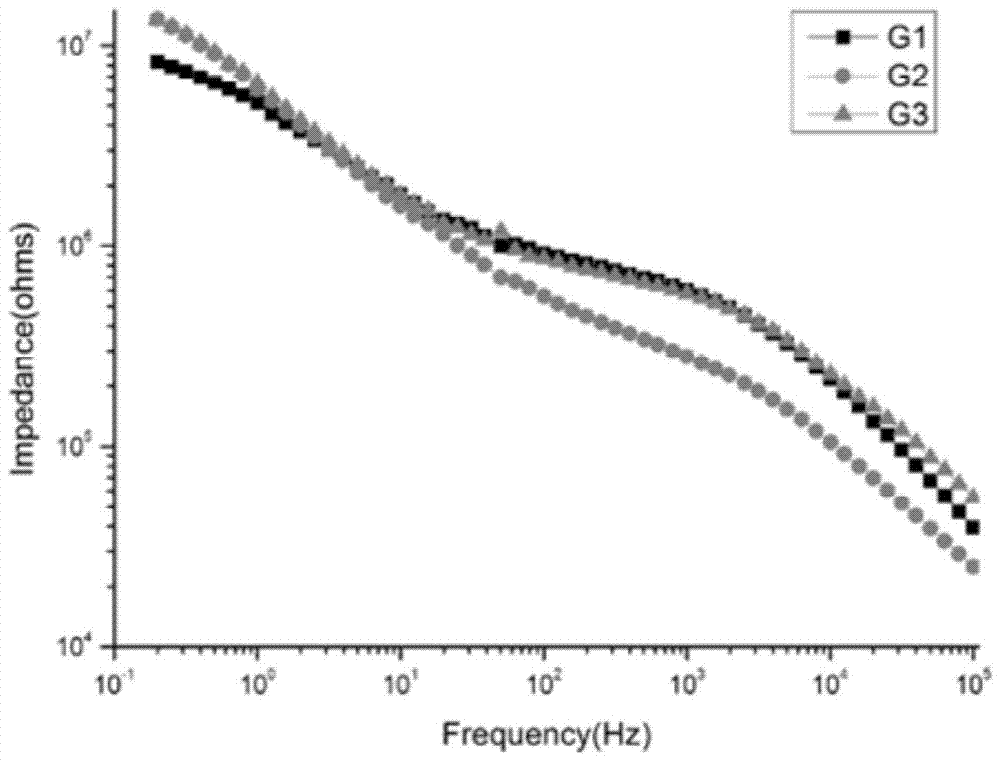
[0028] (4) When performing electrochemical impedance analysis, the electrochemical workstation outputs a sinusoidal AC signal with a peak value of 50mV, and the frequency range is from 0.01HZ to 1MHz.
[00...
Embodiment 3
[0033] Cell culture and detection on a graphene three-dimensional microelectrode array chip
[0034] (1) Surface treatment of the graphene three-dimensional microelectrode array: before inoculating cells, the graphene three-dimensional microelectrode was soaked in 75% ethanol solution for one hour, and then dried under ultraviolet light; then poly-D-lysine (PDL) solution according to 2μg / cm 2 The concentration of 3D microelectrode array was dropped on the surface of the graphene three-dimensional microelectrode array, kept overnight at room temperature, washed three times with ultrapure water, and air-dried.
[0035] (2) Seeding cells on the surface of graphene three-dimensional microelectrode array: Digest conventionally cultured SH-SY5Y cells with digestion solution (0.25% trypsin, 0.02% EDTA solution), centrifuge, pipette, and dilute the cells at 1.0×10 7 cells / mm 3 The density is seeded on the graphene three-dimensional microelectrode array chip.
[0036] (3) Induced di...
PUM
| Property | Measurement | Unit |
|---|---|---|
| impedance | aaaaa | aaaaa |
Abstract
Description
Claims
Application Information


