Manufacturing method for shield type differential via holes and impedance calculation method for differential via holes

A technology of differential vias and fabrication methods, applied in the formation of electrical connection of printed components, electrical components, printed circuits, etc., can solve the problems of discontinuous transmission line impedance, affecting PCB wiring density, signal integrity problems, etc., to meet the needs of high-speed signals. transmission needs, facilitates accurate design and control, resolves the effect of impedance continuity issues

Inactive Publication Date: 2016-04-06
GUANGZHOU FASTPRINT CIRCUIT TECH +2
View PDF5 Cites 7 Cited by
  • Summary
  • Abstract
  • Description
  • Claims
  • Application Information

AI Technical Summary

Problems solved by technology

Differential vias appear as discontinuous breaks in the transmission line impedance on the transmission line, which will cause signal reflection, crosstalk and radiation
The fundamental reason for the impedance discontinuity of the signal via is that there is no reference plane at the via, and the return signal current cannot jump, which increases the inductance of the via, resulting in signal integrity problems
Adding ground holes next to the differential vias can solve this problem, but this method will take up a lot of space, affect the wiring density of the PCB, and cannot accurately design the impedance of the differential vias

Method used


Image

  • Manufacturing method for shield type differential via holes and impedance calculation method for differential via holes
  • Manufacturing method for shield type differential via holes and impedance calculation method for differential via holes
  • Manufacturing method for shield type differential via holes and impedance calculation method for differential via holes

Examples


Embodiment Construction

[0032] Below, in conjunction with accompanying drawing and specific embodiment, the present invention is described further:

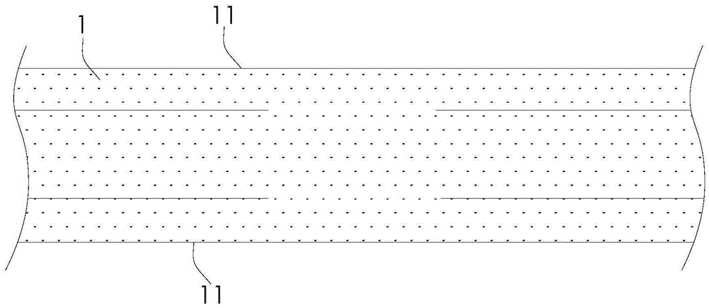
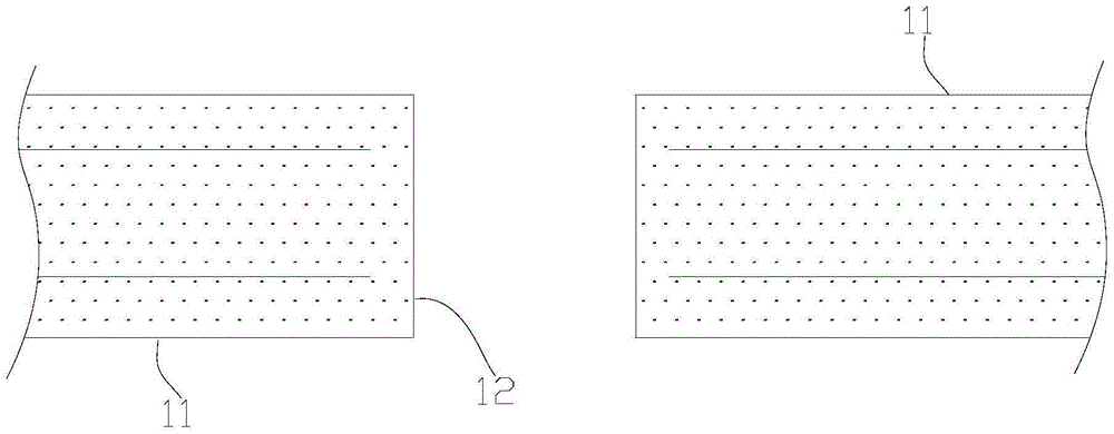
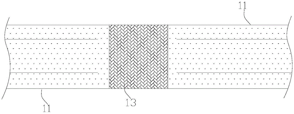
[0033] Such as Figures 1 to 6 As shown, the manufacturing method of the shielded differential via of the present invention includes: setting two reference layers 11 spaced up and down on the insulating medium layer of the PCB board 1; making ground holes 12 on the insulating medium layer of the PCB board 1 , the ground hole 12 is connected to the two reference layers 11; resin 13 is filled in the ground hole 12; a first differential transmission line 141 is arranged above and below the ground hole 12, and a second differential transmission line 141 is arranged above and below the ground hole 12. Differential transmission line 142; two differential signal vias 15 distributed at intervals are made on the PCB 1, the two differential signal vias 15 are located inside the ground hole 12, and the diameter of the differential signal via 15 is smaller than the...


PUM


Abstract

The invention discloses a manufacturing method for shield type differential via holes. The manufacturing method comprises the steps of arranging an upper reference layer and a lower reference layer that are distributed at intervals on an insulating dielectric layer of a PCB; manufacturing a ground hole in the insulating dielectric layer of the PCB, wherein the ground hole is connected with the two reference layers; filling the ground hole with resin; arranging a first differential transmission line above and below the ground hole separately; arranging a second differential transmission line above and below the ground hole separately; and manufacturing two differential signal via holes that are formed at intervals in the PCB. The invention also discloses an impedance calculation method for the differential via holes. The impendence continuity of the differential via holes is realized by the manufacturing method provided by the invention; and in addition, the impendence value of the differential via holes is worked out, so that the accurate design and control for the impendence of the differential via holes can be facilitated.

Description

technical field [0001] The invention relates to a manufacturing method of a shielded differential via hole and an impedance calculation method. Background technique [0002] With the continuous development of communication, cloud computing and cloud storage in the direction of high speed, the signal transmission rate of PCB single channel has gradually increased from 10Gbps to 25Gbps. In the next 3-5 years, the signal transmission rate will further increase to 40-60Gbps. Since the differential line has strong anti-interference advantages, it is widely used in high-speed PCB design. At this time, the differential via design for high-speed differential signal transfer layer is particularly important. [0003] PCB differential vias are conductors that connect different layers of differential signal transmission in a multilayer PCB. Differential vias appear as discontinuous breakpoints in the transmission line impedance on the transmission line, which will cause signal reflecti...

Claims


Application Information

Patent Timeline
Patent Type & Authority Applications(China)
IPC IPC(8): H05K3/42
CPCH05K3/42H05K2201/095
Inventor 王红飞陈蓓邱醒亚
Owner GUANGZHOU FASTPRINT CIRCUIT TECH
Why Eureka
Try Eureka