
An organic light emitting diode device

A light-emitting diode, organic technology, applied in organic semiconductor devices, electrical components, circuits, etc., can solve problems such as poor balance between electrons and holes, degradation of device characteristics, and decrease in efficiency of the light-emitting layer

Active Publication Date: 2016-04-20
LG DISPLAY CO LTD
View PDF3 Cites 16 Cited by
  • Summary
  • Abstract
  • Description
  • Claims
  • Application Information

AI Technical Summary

Problems solved by technology

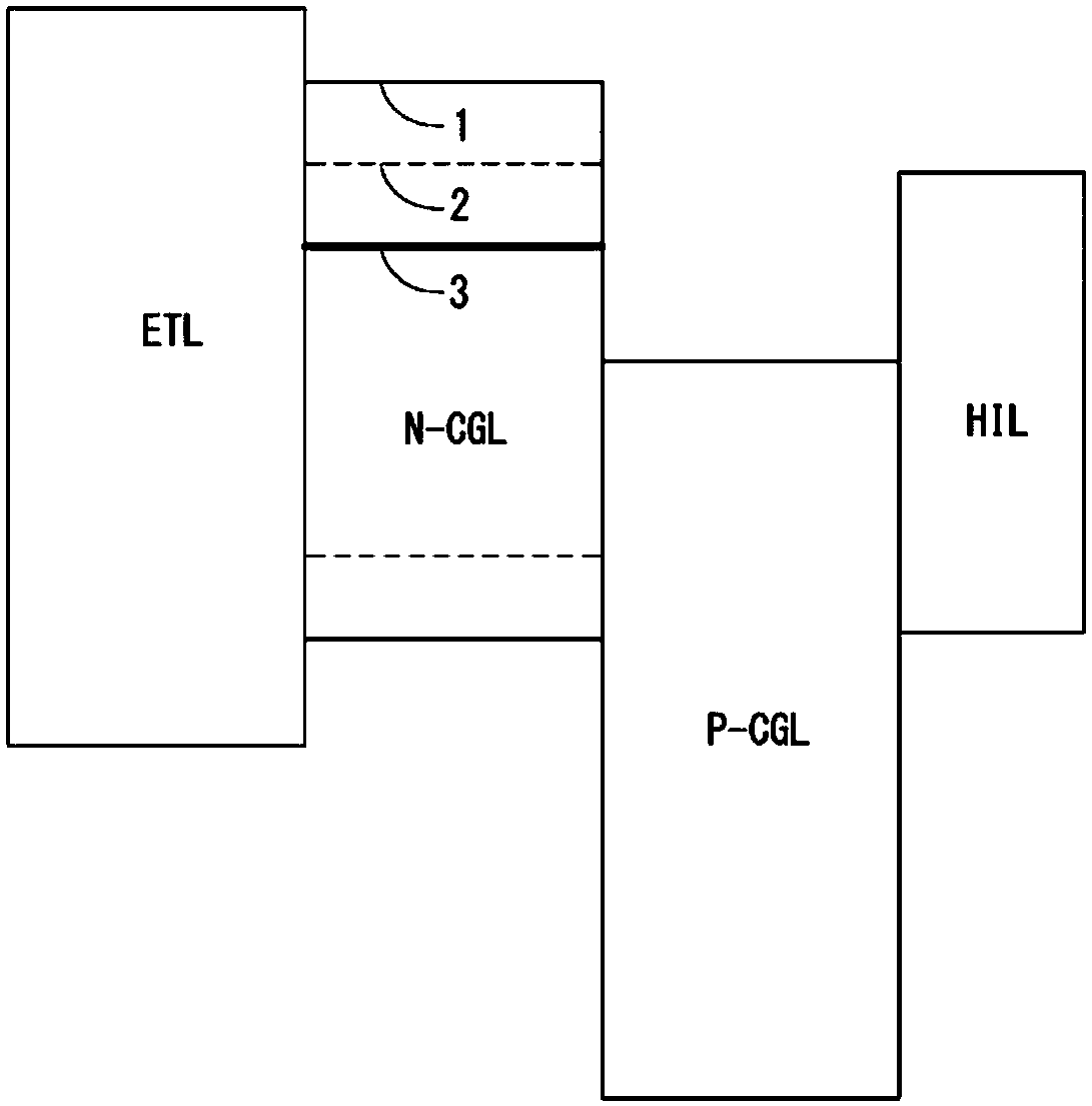
[0006] However, currently used charge generation layers focus on maximizing the injection of holes and electrons into each emissive layer, but are limited in that the transport of electrons from the charge generation layer to the electron transport layer is not smooth
Poor electron injection leads to a poor balance between electrons and holes, resulting in a decrease in the efficiency of the light-emitting layer and thus in the degradation of device characteristics

Method used


Image

  • An organic light emitting diode device
  • An organic light emitting diode device
  • An organic light emitting diode device

Examples


Embodiment approach 1

[0121] An organic light-emitting diode was fabricated using the same composition as in Comparative Example 1 above, except that the host of the N-type charge generation layer was formed of NC-20 compound and phenanthrene compound and doped with 2% Li as a dopant device. The driving voltage, luminous efficiency, and quantum efficiency of the organic light emitting diode devices manufactured according to Comparative Example 1 and Exemplary Embodiment 1 were measured and shown in Table 1 below. Furthermore, the current density with respect to the driving voltage was measured and at Figure 4 As shown in , the emission spectra were measured and at Figure 5 Shown in , the quantum efficiency versus luminance was measured and in Image 6 shown in . (In this case, at 10mA / cm 2 drive the device)

[0122] [Table 1]

[0123]

Driving voltage (V)

Luminous efficiency (Cd / A)

Quantum efficiency (%)

Comparative example 1

7.7

78.4

29.4

Ex...

Embodiment approach 2

[0131] Except that the host of each N-type charge generation layer is formed of NC-20 compound and o-phenanthroline compound and doped with 2% Li as a dopant, organic LED device.

[0132] Driving voltages, luminous efficiencies, and quantum efficiencies of the organic light emitting diode devices manufactured according to Comparative Example 2, Comparative Example 3, and Exemplary Embodiment 2 were measured and shown in Table 2 below. Furthermore, the current density with respect to the driving voltage was measured and at Figure 7 shown in , and measured the quantum efficiency with respect to the brightness of the OLED device and in Figure 8 shown in . (In this case, at 10mA / cm 2 drive the device) Furthermore, the emission spectra of the organic light emitting diode devices manufactured according to Comparative Example 2 and Exemplary Embodiment 2 were measured and obtained at Figure 9 As shown in , the emission spectra of the organic light emitting diode devices manufa...


PUM


Abstract

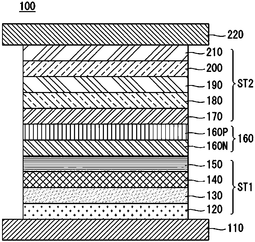
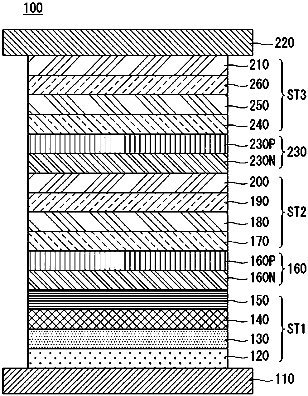
The invention relates to an organic light emitting diode device. The organic light emitting diode device comprises a first light emitting part between an anode and a cathode with the first light emitting part including a first light emitting layer, a second light emitting part comprising a second light emitting layer on the first light emitting part, and a first charge generation layer between the first light emitting part and the second light emitting part, wherein the first charge generation layer comprising at least two hosts, and at least one of the at least two hosts including a pyrene compound.

Description

technical field [0001] The present disclosure relates to an organic light emitting diode device, and more particularly, to an organic light emitting diode device capable of achieving high luminous efficiency and low driving voltage. Background technique [0002] An image display device for displaying various information on a screen is one of the core technologies of the information and communication age. Such image display devices are gradually being developed to be thinner, lighter, more portable and have high performance. With the development of the information society, various demands on display devices are increasing. To meet these needs, flat panel displays such as liquid crystal displays (LCDs), plasma display panels (PDPs), electroluminescence displays (ELDs), field emission displays (FEDs), organic light emitting diodes (OLEDs), etc. Were studied. [0003] Among these flat panel displays, an OLED device is a type of device that emits light as electrons and holes a...

Claims


Application Information

Patent Timeline
Patent Type & Authority Applications(China)
IPC IPC(8): H01L51/50H01L51/54H10K99/00
CPCH10K85/00H10K30/865H10K50/00H10K85/622H10K85/654H10K85/6572H10K50/131H10K2101/90C09K11/06C07D213/02H10K50/13H10K85/626H10K85/633H10K85/636H10K85/6574H10K50/16H10K2102/351
Inventor 姜慧承琴台一丁荣观金亨俊朴正洙
Owner LG DISPLAY CO LTD
Learn More