Laminated organic light emitting diode

An electroluminescent device, an organic technology, applied in the direction of electric solid-state devices, electrical components, semiconductor devices, etc., can solve the problems that technicians cannot obtain technical solutions from this, and achieve the purpose of improving current efficiency and luminous efficiency, improving power efficiency, Effect of High Current Efficiency

Inactive Publication Date: 2014-11-05
KUNSHAN VISIONOX DISPLAY TECH +2
View PDF4 Cites 8 Cited by
  • Summary
  • Abstract
  • Description
  • Claims
  • Application Information

AI Technical Summary

Problems solved by technology

[0006] Although, in theory, increasing the number of electron transport layers or hole transport layers in the connection layer can make the electrons in the electron transport layer undergo level transitions, and it is also mentioned in the above-mentioned documents that the connection layer includes at least one electron transport layer or at least one electron transport layer. Layer hole transport layer or the combination of these layers, but the prior art including the above-mentioned documents have no structure, material selection and effect of the connecting layer with multi-layer electron transport layer or multi-layer hole transport layer, etc. Make any specific instructions so that those skilled in the art cannot obtain feasible technical solutions

Method used


Image

  • Laminated organic light emitting diode
  • Laminated organic light emitting diode
  • Laminated organic light emitting diode

Examples


Embodiment 1

[0082] In this embodiment, an ITO conductive glass substrate with a specific pattern etched is used as the substrate, and the substrate is ultrasonically cleaned in deionized water containing a cleaning solution. The temperature of the cleaning solution is about 60°C, and then infrared baking is used. The lamp bakes the cleaned substrate, and puts it into the evaporation chamber to evaporate the anode layer, a number of the light-emitting unit layers (and the connection between adjacent light-emitting unit layers). Layer) and the cathode layer, the chamber pressure during the evaporation process is lower than 1.0×10⁻³Pa.

[0083] The device structure is:
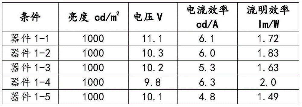
[0084] Device 1-1:

[0085] ITO / NPB(80nm) / EL / N1 / N2 / P1 / EL / Alq 3 (30nm) / LiF(0.5nm) / Al(150nm)

[0086] Device 1-2:

[0087] ITO / NPB(80nm) / EL / N1 / N2 / N3 / P1 / EL / Alq 3 (30nm) / LiF(0.5nm) / Al(150nm)

[0088] Devices 1-3:

[0089] ITO / NPB(80nm) / EL / N1 / N2 / N3 / N4 / P1 / EL / Alq 3 (30nm) / LiF(0.5nm) / Al(150nm)

[0090] Devices 1-4:

[0091] ITO / NPB(80nm) / EL / N1(...

Embodiment 2

[0118] The processing process of this embodiment is similar to the first embodiment.

[0119] The device structure is:

[0120] Device 2-1:

[0121] ITO / NPB(80nm) / EL / N1 / N2 / P1 / EL / Alq 3 (30nm) / LiF(0.5nm) / Al(150nm)

[0122] Device 2-2:

[0123] ITO / NPB(80nm) / EL / N1 / N2 / N3 / P1 / EL / Alq 3 (30nm) / LiF(0.5nm) / Al(150nm)

[0124] Device 2-3:

[0125] ITO / NPB(80nm) / EL / N1 / N2 / N3 / N4 / P1 / EL / Alq 3 (30nm) / LiF(0.5nm) / Al(150nm)

[0126] The above-mentioned device 2-1 is a device structure of the prior art, which is a comparative example of the second embodiment; and the device 2-2 and the device 2-3 are the device structures proposed by the present invention. The specific structures and materials of the above device 2-1, device 2-2, and device 2-3 are described in detail as follows:

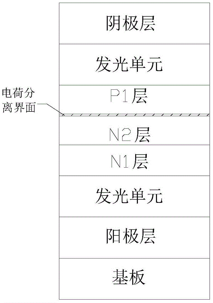
[0127] Device 2-1 is an existing device structure, and its connection layer includes two electron transport layers (N1 and N2) and a hole transport layer (P1), namely N1 / N2 / P1 layer structure, N1 / N2 / P1 layer Connect the two light-em...

Embodiment 3

[0148] The processing process of this embodiment is similar to the first embodiment.

[0149] The device structure is:

[0150] Device 2-2:

[0151] ITO / (NPB80nm) / EL / N1 / N2 / N3 / P1 / EL / Alq 3 (30nm) / LiF(0.5nm) / Al(150nm)

[0152] Device 2-4:

[0153] ITO / (NPB80nm) / EL / N1 / N2 / N3 / P1 / EL / Alq 3 (30nm) / LiF(0.5nm) / Al(150nm)

[0154] Among them, the device 2-2 is the same as the second embodiment.

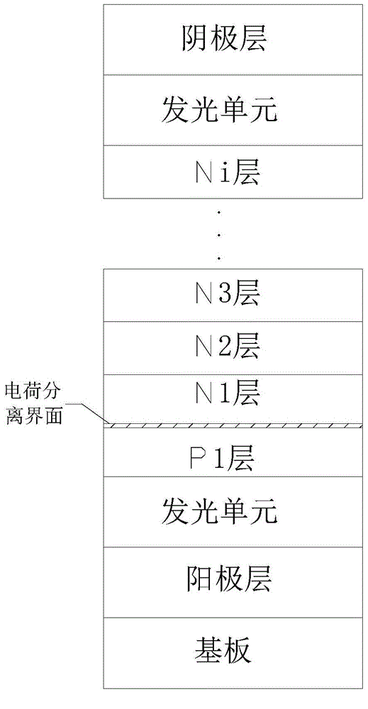
[0155] The connection layer of device 2-2 has three electron transport layers (N1, N2 and N3) and one hole transport layer (P1), namely N1 / N2 / N3 / P1 layer structure, N1 / N2 / N3 / P1 layer Connect the two light-emitting unit layers in series, and the two light-emitting unit layers EL are single-layer luminescent Alq 3 . among them:

[0156] Electron transport layer N1, using Alq 3 :Li, thickness is 30nm, of which Alq 3 The LUMO energy level is 3.1eV;

[0157] The electron transport layer N2 uses PTCBI with a thickness of 2nm and a LUMO energy level of 4.1eV;

[0158] The electron transport layer N3 uses a HAT with a...


PUM


Abstract

The invention discloses a laminated organic light emitting diode which comprises a substrate, as well as an anode layer, a plurality of light emitting unit layers and a cathode layer which are sequentially formed on the substrate, wherein a connection layer is arranged between every two adjacent light emitting unit layers and is in an at least four-layer structure which comprises at least three electronic transmission layers and a hole transmission layer; the thicknesses of the electronic transmission layers and the hole transmission layers are 1-100nm; a charge separation interface is arrange on a surface, contacted with each hole transmission layer, of the electronic transmission layer; the electronic transmission layers forming the charge separation interfaces are made of organic materials with LUMO (Lowest Unoccupied Molecular Orbital) energy levels higher than 5.0eV or inorganic materials with conduction band levels of 5.5-6.5eV; and the hole transmission layers forming the charge separation interfaces are made of organic materials with HOMO (Highest Occupied Molecular Orbital) energy levels not higher than 5.7eV. According to the device, appropriate middle energy level layers are arranged between the charge separation interfaces and the light emitting unit layers, a transition potential barrier is reduced, and driving voltage of the laminated device is reduced, so that higher current efficiency is obtained.

Description

Technical field [0001] The invention relates to the technical field of organic electroluminescence devices, in particular to a laminated organic electroluminescence device. Background technique [0002] Organic electroluminescence refers to the phenomenon that organic light-emitting materials emit light under the excitation of electric current or electric field. Organic Light Emitting Diode (Organic Light Emitting Diode, hereinafter referred to as OLED) is a device that uses an organic material as an active light-emitting layer under the action of an electric field. In recent years, OLED has attracted widespread attention due to its thin shape, high brightness, fast response, wide viewing angle, simple process, and flexibility. It has important applications in the field of display and lighting and has become a very popular emerging at home and abroad. Flat panel display industry. [0003] In order to obtain high current efficiency and long working life, people have designed stack...

Claims


Application Information

Patent Timeline
Patent Type & Authority Applications(China)
IPC IPC(8): H01L51/50H01L51/54
CPCH10K50/11H10K2101/40H10K50/131H10K50/166H10K50/15
Inventor 邱勇张国辉段炼
Owner KUNSHAN VISIONOX DISPLAY TECH
Why Eureka
Try Eureka