Nonvolatile memory device and manufacturing method thereof

A non-volatile, manufacturing method technology, applied in semiconductor/solid-state device manufacturing, electrical solid-state devices, semiconductor devices, etc., can solve problems such as degradation, electrical performance failure of non-volatile memory devices, and reduce manufacturing costs , improve product yield, and solve the effect of performance degradation

Active Publication Date: 2016-04-27
WINBOND ELECTRONICS CORP
View PDF3 Cites 4 Cited by
  • Summary
  • Abstract
  • Description
  • Claims
  • Application Information

AI Technical Summary

Problems solved by technology

[0005] The object of the present invention is to provide a non-volatile memory device and a manufacturing method thereof, so as to improve the failure or deterioration of the electrical performance of the non-volatile memory device

Method used


Image

  • Nonvolatile memory device and manufacturing method thereof
  • Nonvolatile memory device and manufacturing method thereof
  • Nonvolatile memory device and manufacturing method thereof

Examples


Embodiment Construction

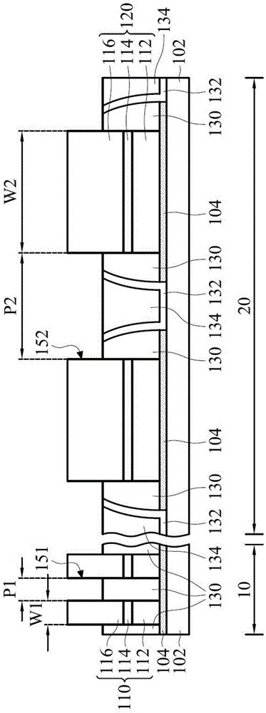
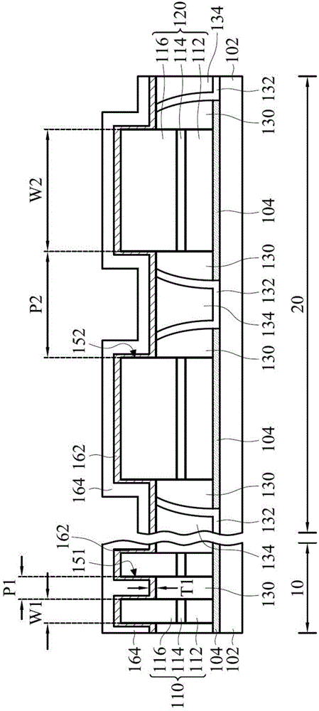
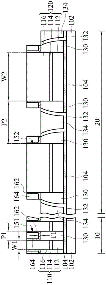
[0037] The invention provides a non-volatile memory device and a manufacturing method thereof, Figure 1A to Figure 1F It is a schematic cross-sectional view illustrating various manufacturing process stages of forming a non-volatile memory device 100 according to some embodiments of the present invention.

[0038] Please refer to Figure 1A , providing a substrate 102 including an array area 10 and a peripheral circuit area 20 adjacent to the array area 10 . A plurality of first polysilicon gate stack structures 110 may be formed on the substrate 102 of the array region 10 , and a plurality of second polysilicon gate stack structures 120 may be formed on the substrate 102 of the peripheral circuit region 20 .

[0039] In some embodiments, the material of the substrate 102 may include silicon, gallium arsenide, gallium nitride, germanium silicide, silicon-on-insulator (SOI), other suitable materials, or a combination of the above materials.

[0040] The fabrication of the fir...


PUM


Abstract

The invention provides a nonvolatile memory device and a manufacturing method thereof. The manufacturing method of the nonvolatile memory device comprises the step of: providing a substrate comprising an array region; forming at least two polycrystalline silicon gate stack structures on the array region of the substrate; forming an insulating layer between the at least two polycrystalline silicon gate stack structures, wherein a groove is formed in the insulating layer between the at least two polycrystalline silicon gate stack structures; forming a first metal layer on the side walls and the bottom part of the groove; filling a protective layer in the groove to cover the first metal layer; and forming a second metal layer on the top part surfaces of the at least two polycrystalline silicon gate stack structures and the protective layer, so that the protective layer is surrounded by the first metal layer and the second metal layer. The metal layer provided by the invention can effectively solve the problems of performance degradation and electrical property failure of the nonvolatile memory device.

Description

technical field [0001] The present invention relates to a semiconductor storage device, and in particular to a non-volatile memory device and a manufacturing method thereof. Background technique [0002] In non-volatile memory, according to whether the data in the memory can be rewritten at any time when using a computer, it can be divided into two types of products, namely read-only memory (ROM) and flash memory (flash memory). Among them, the flash memory has gradually become the mainstream technology of the non-volatile memory due to its low cost. [0003] In some existing techniques for forming a polysilicon gate stack structure by performing metal silicidation reaction between silicon and a metal layer, only one deposition process is performed to conformably form a metal layer and a protection layer on the polysilicon gate stack structure. However, if the thickness of the metal layer is too large, the metal silicide will remain between adjacent polysilicon gate stack s...

Claims


Application Information

Patent Timeline
Patent Type & Authority Applications(China)
IPC IPC(8): H01L27/115H01L21/8247H01L27/11521
Inventor 杨政达
Owner WINBOND ELECTRONICS CORP
Why Eureka
Try Eureka