A kind of semiconductor laser and its manufacturing method

A manufacturing method and laser technology, applied to semiconductor lasers, lasers, laser components, etc., can solve the problems of high manufacturing cost, complicated manufacturing process, and limited power, and achieve low manufacturing cost, mature technology, and suppression of high-order modes the effect of

Active Publication Date: 2018-10-19
CHANGCHUN INST OF OPTICS FINE MECHANICS & PHYSICS CHINESE ACAD OF SCI
View PDF5 Cites 0 Cited by
  • Summary
  • Abstract
  • Description
  • Claims
  • Application Information

AI Technical Summary

Problems solved by technology

[0005] However, compared with the traditional semiconductor laser, the semiconductor laser with the above structure has the problems of complicated manufacturing process, high manufacturing cost or limited power.

Method used


Image

  • A kind of semiconductor laser and its manufacturing method
  • A kind of semiconductor laser and its manufacturing method
  • A kind of semiconductor laser and its manufacturing method

Examples


Embodiment Construction

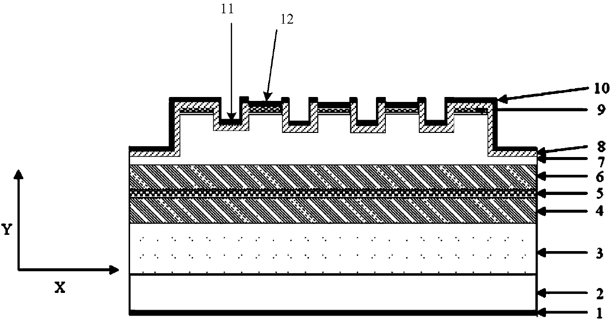
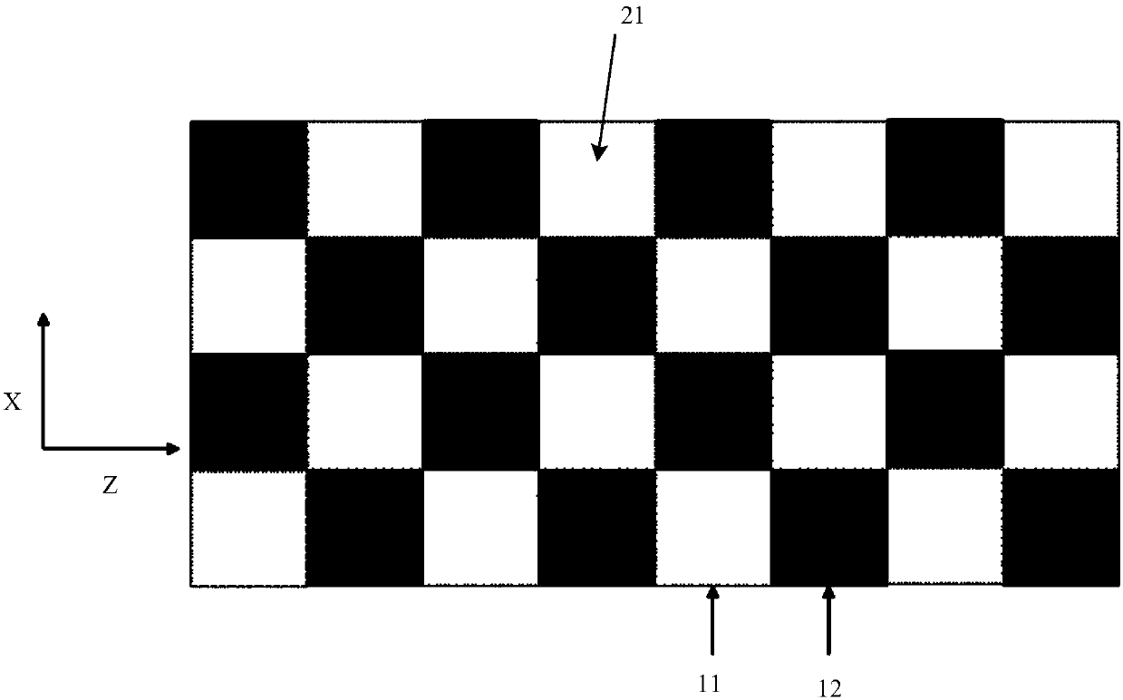
[0041] The following will clearly and completely describe the technical solutions in the embodiments of the present invention with reference to the accompanying drawings in the embodiments of the present invention. Obviously, the described embodiments are only some, not all, embodiments of the present invention. Based on the embodiments of the present invention, all other embodiments obtained by persons of ordinary skill in the art without making creative efforts belong to the protection scope of the present invention.

[0042] As mentioned in the background technology, in order to reduce the lateral divergence angle of semiconductor lasers, semiconductor lasers with structures such as unstable resonators, a-DFB lasers, tapered lasers, and tilted cavity lasers have complex manufacturing processes compared to traditional semiconductor lasers. , High production cost or limited power.

[0043] Therefore, how to reduce the lateral divergence angle of the semiconductor laser while ...


PUM


Abstract

The invention discloses a semiconductor laser and a manufacturing method thereof. The semiconductor laser includes: an N-type electrode and a P-type electrode arranged oppositely; a functional layer arranged between the N-type electrode and the P-type electrode; In one direction, the functional layer includes a substrate, an N-type cladding layer, an N-type optical confinement layer, an active region, a P-type optical confinement layer, a P-type cladding layer, an insulating layer, and a P-type ohmic contact layer arranged in sequence; Wherein, the first direction is the direction from the N-type electrode to the P-type electrode; the P-type electrode includes: a current injection region and a non-current injection region; in the first direction, the insulating The position of the layer opposite to the current injection region is provided with a hollow pattern, so that the P-type electrode and the P-type ohmic contact layer are electrically connected at the current injection region. The semiconductor laser is characterized by a low lateral divergence angle.

Description

technical field [0001] The invention relates to the technical field of semiconductor devices, and more specifically, to a semiconductor laser and a manufacturing method thereof. Background technique [0002] Semiconductor lasers are widely used in fields such as medical treatment, display, communication, material processing, and pumping solid-state lasers due to their small size, light weight, and high conversion efficiency. With the continuous expansion of application fields, people put forward higher and higher requirements for the power and beam quality of semiconductor lasers. [0003] By optimizing the epitaxial structure design and improving material growth, the fast-axis divergence angle of semiconductor lasers has been greatly improved. The improvement of the output power of semiconductor lasers can be achieved by wide-strip electrical contact, but this structure makes the quality of the lateral output beams of semiconductor lasers poor, and the external characteris...

Claims


Application Information

Patent Timeline
Patent Type & Authority Patents(China)
IPC IPC(8): H01S5/343H01S5/24
CPCH01S5/24H01S5/34353H01S5/3438H01S5/34386
Inventor 佟存柱王涛汪丽杰田思聪舒世立张建王立军
Owner CHANGCHUN INST OF OPTICS FINE MECHANICS & PHYSICS CHINESE ACAD OF SCI
Why Eureka
Try Eureka